• Please review our updated Terms and Rules here

The Digicos PDP8 Super-MMU

jdreesen

Experienced Member
Joined
Jul 5, 2012
Messages
443
Location
Switzerland
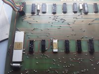
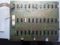
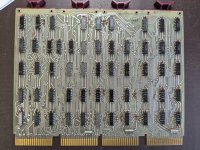
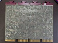
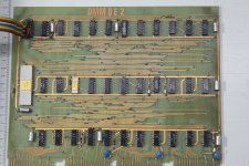
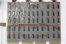
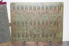
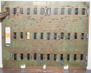
I have a very special, extended version of the M837 : the extension itself is a complete omnibus board with a single AMD2901. From the description found in Bitsavers :

Finally the super MNemory Management Unit for the PDP8 is here!
This piece of ingenious hardware replaces and extends the Memery Extension
Control (KM8E or KH8-AA) and provides the capabilities necessary to run
foreground/background systems like RTS-8 and MULTIS at full speed. It can
be considered a major extension to the PDP8 architecture.
The new unit consists of two modules that plug into the Omnibus replacing
the memory extension control. It provides two extra functions, dynamic
instruction trapping en dynamic field relocation.


Pics :
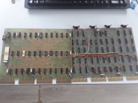
20241002_113953.jpg


20241002_115835.jpg
20241002_115858.jpg


It is available for a true hardcore PDP8 enthusiast, (i.e. not a hoarder...) as I will never get around to using it.
BUT : I need a M837 in return ( as I need to keep my PDP8 complete.)
Located in Switzerland.
 

Attachments

  • 20241002_115835.jpg
    20241002_115835.jpg
    2.6 MB · Views: 26
Well, you've got my attention! Is there any documentation for it?

I read mentions in the MULTI8 manual (which seems to suggest they eventually got it down to one board), and in various newsletters. I did not find the bitsavers document you quoted, though.
 
It looks like one of the boards does not have plated holes, but instead has had the vias manually completed with wire and solder.
It looks to me like someone took an M837 module, did some rework, and added domr bodge wires (ribbon cable) over to their board. Their board looks like they were etching it themselves or something. Which makes some sense, as I understand these were a bit experimental and never made in large quantity.

I found a fair bit of info in the Vandermark website, but mostly from the perspective of the MULTI8 software. I'd love to see some information about the hardware used to implement that specification.

Later today I'll see if I can test a spare M837.
 
Hmm. Both of my M837 work fine for booting OS/8, but the diagnostic crashes at location 0001 on both. So perhaps there's an issue, or perhaps my copy of DHMCAB is corrupt.

I started looking at what it would take to reverse engineer the thing. I think I found cross reference information for M11 and probably GX, but not the Intel M15 chip. Anybody know what that is?

Also, the rightmost two chips on the bottom row and the fourth chip from the right in the top row are illegible to me. Can you tell me what their markings are?
The two rightmost ICs on the bottom row are both Signetics N8325B. The fourth IC from the right in the top row is a DEC7400N.

Here are full resolution photos of both sides just in case you need more details:

PXL_20241005_050601794.jpg

PXL_20241005_050453232.jpg
 
Hmm. Both of my M837 work fine for booting OS/8, but the diagnostic crashes at location 0001 on both. So perhaps there's an issue, or perhaps my copy of DHMCAB is corrupt.

...

Sounds like this might be an un-handled interrupt. Check location zero for the PC of the location in DHMCAB where the interrupt occurred.
 
The two rightmost ICs on the bottom row are both Signetics N8325B. The fourth IC from the right in the top row is a DEC7400N.

Here are full resolution photos of both sides just in case you need more details:
I'm sorry, I meant for those questions to refer to the Dicigos board. I've got a couple of M837 to study. Thanks!
 
I will put up some more detailed pic today, but for now :
 

Attachments

  • IMG_5250.JPG
    IMG_5250.JPG
    7.6 MB · Views: 14
  • IMG_5246.JPG
    IMG_5246.JPG
    7.4 MB · Views: 14
  • IMG_5214.JPG
    IMG_5214.JPG
    7.4 MB · Views: 14
Last edited:
I think I found cross reference information for M11 and probably GX, but not the Intel M15 chip. Anybody know what that is?
Attached is my marked up DMM8E2 pic with chip reference numbers in the typical DEC sequence. Also my list of what types are used.
I agree the M11 and GX are Mullard chips (although the M11 in the top row seems to show a TI logo). The M15 (E26) is a mystery at this point. If it didn't have the i logo, I'd guess it could be another Mullard chip.

The latest pics from jdreeson help identify some of the chips. E4 is a SP380A and E15 is a 7404.
 

Attachments

  • DMM8E2-3-ic.jpg
    DMM8E2-3-ic.jpg
    2.5 MB · Views: 7
  • DMM8E2-IC.txt
    533 bytes · Views: 6
Last edited:
E1 is a 7401.
E18 is indeed strange, with a TI740x stamped before the Mullard M11. And it has 16 pins, wich no SN740x has.

Where did you find Mullard xref info ?
 
Last edited:
Where did you find Mullard xref info ?
I've been speculatively following an assumption that the Mullard and Intel chips have been re-marked by ICL.


Alas, that doesn't tell me what an M15 is. I'm assuming the GX is the "H" version of the 7440, similarly to how the FX relates to the F.
 
I have now confirmed that I have one working M837, but the other isn't quite working right.

I also started puttering with the reverse engineering -- mostly the connections to the DATA and MD busses in the bottom row of ICs.
 
Back
Top