Hugo Holden
Veteran Member
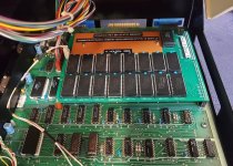
I have been doing some work lately making a non-volatile memory board for my PET. It plugs onto the Dynamic PET's board J4 & J9 and has two additional wires which connect it to the pcb. One is for the 5V power, the other to inhibit DRAM reads. The non-volatile memory then is the one in use.
I wanted to make this board out of period correct parts for the PET (my usual M/O in the spirit of vintage computing). I decided to go with battery backed up SRAM.
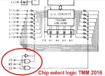
There are some very interesting issues that can occur trying to achieve this. They relate to the conditions of the RAM control signals during power up and power down/power failure events. Not only are the address & data lines transiently unstable and indeterminate, but also the chip enable signals including the write control too.
Dallas solved this problem to a good degree with an SRAM controller IC inside their battery backed up SRAM memories. Also one assumption that is made for other non-volatile RAMs is that the power up process is not as problematic, if the CPU is in reset and the write and/or chip select controls are tri-stated and tied high and they follow the rise in power supply voltage and don't cause trouble. However, for any specific computer that assumption may not apply.
I decided to inspect the write control in the PET with the slow scan/storage scope. The +5V power (on both regulators) rises fairly abruptly at power on, and there is a very early write transient. This would corrupt the non volatile memory . At power down , the +5v supply decays over about 100mS with an inverted exponential form and there is a very nasty early write transient in the R/W control line by the time the voltage has dropped to the region of 3v.
Therefore I designed two custom circuits, to deal with these in the PET, using vintage LM111 comparators, so as to eliminate these from the write control signal. The memory contents are then not corrupted by computer power on/off events.
The battery can support the memory for well over 1 year, I decided to use a cordless phone twin AAA style rechargeable battery and there is a battery charge and power-up down system with 4 transistors. This is the battery management system used on the Yang S-100 32k memory board.
Yang used an interesting approach to help preserve the memory contents on power cycling, he interfaced the memory IC's with a number of cmos peripheral chips and powered those from the backed up battery supply, so that the events of power cycling did not corrupt the memory. It resulted in more standby power consumption though and the system would not help the PET's unique case.
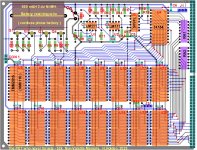
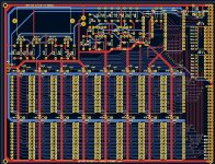
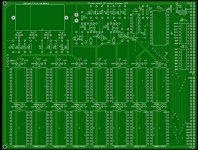
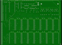
I'm still experimenting with this project. The top & bottom pcb foil patterns are finished.
I wanted to make this board out of period correct parts for the PET (my usual M/O in the spirit of vintage computing). I decided to go with battery backed up SRAM.
There are some very interesting issues that can occur trying to achieve this. They relate to the conditions of the RAM control signals during power up and power down/power failure events. Not only are the address & data lines transiently unstable and indeterminate, but also the chip enable signals including the write control too.
Dallas solved this problem to a good degree with an SRAM controller IC inside their battery backed up SRAM memories. Also one assumption that is made for other non-volatile RAMs is that the power up process is not as problematic, if the CPU is in reset and the write and/or chip select controls are tri-stated and tied high and they follow the rise in power supply voltage and don't cause trouble. However, for any specific computer that assumption may not apply.
I decided to inspect the write control in the PET with the slow scan/storage scope. The +5V power (on both regulators) rises fairly abruptly at power on, and there is a very early write transient. This would corrupt the non volatile memory . At power down , the +5v supply decays over about 100mS with an inverted exponential form and there is a very nasty early write transient in the R/W control line by the time the voltage has dropped to the region of 3v.
Therefore I designed two custom circuits, to deal with these in the PET, using vintage LM111 comparators, so as to eliminate these from the write control signal. The memory contents are then not corrupted by computer power on/off events.
The battery can support the memory for well over 1 year, I decided to use a cordless phone twin AAA style rechargeable battery and there is a battery charge and power-up down system with 4 transistors. This is the battery management system used on the Yang S-100 32k memory board.
Yang used an interesting approach to help preserve the memory contents on power cycling, he interfaced the memory IC's with a number of cmos peripheral chips and powered those from the backed up battery supply, so that the events of power cycling did not corrupt the memory. It resulted in more standby power consumption though and the system would not help the PET's unique case.
I'm still experimenting with this project. The top & bottom pcb foil patterns are finished.
Attachments

Last edited:
") ...
...