ardent-blue
Veteran Member
- Joined
- Jan 1, 2015
- Messages
- 686
Folks, I am getting curbstomped. I have been trying to develop the grand unification theory for PS/2 Configuration Memory varieties, got the RTCs, external NVRAM [SRAM], and the devil cursed RTC Modules [like the DS1287] identified by system.
Plenty of published stuff on accessing the defined registers in the RTC. It seems that writing to / reading from the SRAM portion of an RTC [aka "CMOS"] or ritin'/readin' the external SRAM [aka "NVRAM" or "Extended CMOS"] is done to addresses, not registers.
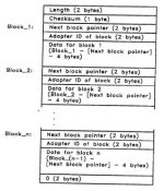
WHAT is the form of the header? This was complexified when IBM dreamed up the NVRAM Dynamic Data Area in early 1990 [only a partial TDB...]. Note that the block is NOT of a fixed length anymore. How is this set up?

Function: 09h — Write to CMOS RAM from the ABIOS seems to resemble a structure, but this may be the older one. Also, looking [confuzedly] at the Undocumented PC, 2d Ed. Wondering if the utilities only support 2k and 8k NVRAM, while there are a few 4k implementations out there [8553 and 8555LS ?]. It would not strike me as impossumble for one of these rare 4k systems to bring the CMOSVIEW utility to a smoke-belching stop.
I did not sleep at a Holiday Inn Express last night... MAJ Tom has divulged some details, but the 95 Tech Ref only concerns itself with the CMOS, no mention of Extended CMOS.
NOTE: While czeching each model's page to verify the RTC / NVRAM chipset, I noticed that while the 25MHz 8580 Type 3 system board uses the Motorola MC146818AFN RTC/CMOS, it also uses the Sanyo LC3664NML-12 8Kx8 SRAM. Only 8570 or 8580 to use the combo. All others use 2kx8 SRAM.
Plenty of published stuff on accessing the defined registers in the RTC. It seems that writing to / reading from the SRAM portion of an RTC [aka "CMOS"] or ritin'/readin' the external SRAM [aka "NVRAM" or "Extended CMOS"] is done to addresses, not registers.
WHAT is the form of the header? This was complexified when IBM dreamed up the NVRAM Dynamic Data Area in early 1990 [only a partial TDB...]. Note that the block is NOT of a fixed length anymore. How is this set up?

Function: 09h — Write to CMOS RAM from the ABIOS seems to resemble a structure, but this may be the older one. Also, looking [confuzedly] at the Undocumented PC, 2d Ed. Wondering if the utilities only support 2k and 8k NVRAM, while there are a few 4k implementations out there [8553 and 8555LS ?]. It would not strike me as impossumble for one of these rare 4k systems to bring the CMOSVIEW utility to a smoke-belching stop.
I did not sleep at a Holiday Inn Express last night... MAJ Tom has divulged some details, but the 95 Tech Ref only concerns itself with the CMOS, no mention of Extended CMOS.
NOTE: While czeching each model's page to verify the RTC / NVRAM chipset, I noticed that while the 25MHz 8580 Type 3 system board uses the Motorola MC146818AFN RTC/CMOS, it also uses the Sanyo LC3664NML-12 8Kx8 SRAM. Only 8570 or 8580 to use the combo. All others use 2kx8 SRAM.
Last edited:
