• Please review our updated Terms and Rules here

TRS-80 diagnostic/ICE card

David,
But, even without the LC Mod it should still display the characters that are in the Character Generator. The Level II
Manual gives these as the Characters:.


Larry


Model-1_Char_Gen.jpg8046670.jpg
 
David,
But, even without the LC Mod it should still display the characters that are in the Character Generator. The Level II
Manual gives these as the Characters:.


Larry


View attachment 45885View attachment 45886

I assumed it would which is why it had lower case to start with, not having a functioning model 1 or a an image of what characters are wrong I can only guess.
 
OK, I've had a chance to get back to the diagnostic ROMs.

This is a G board with no lower case. The first picture shows that the characters are not correct, in some locations. This happens in both David's version and Larry's version (since they are based on the same code).

On a D board, with lower case, everything displays as it should.

The second picture shows Larry's ROM with the characters all converted to upper case. When plugged in, it shows all @9 which tells me there is something wrong with the code. I burned it twice and got the same thing both times.

The third picture shows Larry's keyboard scan diagnostic and it seems to work right. Unfortunately, none of the Model 1s I have that are working enough to show something intelligent on the screen don't have keyboard issues. I do have some Model 1 motherboards that have no keyboard attached and I'm guessing the ROM will see that as an issue. :)
 

Attachments

  • IMG_20180609_113611.jpg
    IMG_20180609_113611.jpg
    79.5 KB · Views: 3
  • IMG_20180609_113944.jpg
    IMG_20180609_113944.jpg
    83.6 KB · Views: 2
  • IMG_20180609_114351.jpg
    IMG_20180609_114351.jpg
    82.1 KB · Views: 3
OK, in the first picture (G Board with NO Lowercase), the first line should be:

Komtek Test ROM Version 1.4a

Instead you are getting the following HEX values:
K= Correct
o= 4F or 6F / =2F <-- This is telling me there is some problem with the Data Lines such that a 4F is converted to 2F for the Video Display.
m= 4D or 6D - =2D
t= 54 or 74 4 =34
e= 45 or 65 % =25
k= 4B or 6B + =2B
= Correct
T= Correct
e= 45 or 65 % =25
s= 53 or 73 3 =33
t= 54 or 75 4 =34
= Correct
R= Correct
O= Correct
M= Correct
= Correct
V= Correct
e= 45 or 65 % =25
r= 52 or 72 2 =32
s= 53 or 73 3 =33
i= 49 or 69 ) =29
o= 4F or 6F / =2F
n= 4E or 6E . =2E
= Correct
1= Correct
.= Correct
4= Correct
a= 41 or 61 ! =21

I am curious why the Case Conversion ROM gives @9's on the screen versus the same information as the Lowercase version. Especially since
it works correct in my Emulator. I've got to dig out my Model 1 and repair it so I can also test it.

The Keyboard test ROM just echo's on the screen what key is shorted ROW to COLUMN. It doesn't test the existence of a keyboard as that is
just a Hardware matrix of switches at 0x3800.

Thanks.

Larry
 
Display Problem

Display Problem

If you look at the attached PNG, and follow Pin 12 of Z62 down to Z28 that is the Bit that is 2 of 1,2,4,8.
Then follow Pin 12 of Z45A for Lower Case Modified Motherboards, or Pin 13 of Z30 down to Pin 13 of Z27,
that is Bit 4 of 1,2,4,8 for the MSD. It appears that there is some type of Wiring Wiring error for Pin 10
of Z28 to be selected when Pin 15 of Z27 should be selected (Input is Pin 13 (D3) of Z27).

No way that one bad IC Z27 or Z28 can set the Bit in the other IC unless Pin 12 of Z62 (Bit 5) is some how
shorted to Pin 13 of Z30.

It will be interesting to see what you find.

Thanks.

Larry

Model-1_Lowercase_Mod.jpg
 
The display is how it should be according to the schematic for a Model1 with no LC Mod.

Take a lower case "o" as an example. Its value is 6Fh, the bit of importance is D5, it feeds into a Z30 a 74LS02 (NOR Gate). The input in this case is high, the output of that gate which is now low is latched and fed into the character generators A6 input. So the character being fed into the character generator is now 2F.

An upper case "O" (4Fh) D5 is low which is inverted via the NOR gate and fed into A6 (high) effectively inputting 4Fh to the character generator.

All I can say is its an ugly way to reduce the chip count by one static RAM.

So what it means is for machines with no LC mod the bit swapping they do means lower case wont display correctly. Adding a code to test for the absence of an LC mod and using a different set of upper case only messages will overly complicate the code.
The best solution is to only use upper case messages.
 
Last edited:
All I can say is its an ugly way to reduce the chip count by one static RAM.

So what it means is for machines with no LC mod the bit swapping they do means lower case wont display correctly. Adding a code to test for the absence of an LC mod and using a different set of upper case only messages will overly complicate the code.
The best solution is to only use upper case messages.

FWIW there's a fairly simple way to handle printing messages and having them uppercased on Model I's without the lower-case mod. I seem to recall finding the technique when disassembling Big Five games. With HL pointing to screen memory and A containing the character to print, do this:
Code:
    LD   (HL),A
    CP   (HL)
    JR   Z,chok
    RES  5,(HL)
chok:
 
Unfortunately its not that simple for the ROM. To make the ROM code able to function in a system with faulty or no RAM, we can't use the stack. Normally it would be a simple matter of testing for the existence of an LC mode storing the result and adding your code example to a single display subroutine. But since we cant use a memory variable or a subroutine all temporary variables have to be held in registers and each time we display a message it is hard coded not in a subroutine. Hard coding an LC test and the conversion 10 or 15 times versus not using lower case... the choice is simple.

FWIW there's a fairly simple way to handle printing messages and having them uppercased on Model I's without the lower-case mod. I seem to recall finding the technique when disassembling Big Five games. With HL pointing to screen memory and A containing the character to print, do this:
Code:
    LD   (HL),A
    CP   (HL)
    JR   Z,chok
    RES  5,(HL)
chok:
 
Things seem to have gotten side tracked with the test ROM I wrote but I have been focused on the original goal.

After laying out a few schematics in KiCAD I've settled on a solution based around an Arduino Mega2560. There is an existing project that has a few limitations with DRAM tests not being reliable because the RAS/MUX/CAS sequence are generated based on a clock source the ICE has no access to.

Connecting to the expansion interface works around that problem because the ICE has to provide those signals. I've put together a schematic that builds on the other project but provides the ability to connect via the cpu socket or the expansion connector.
I can detect in the software when the expansion interface cable is connected and automatically adapt the operation to whichever interface is being used.

The cpu connection will work with the standard software from the other project, I'll be writing extensions to the code to support the expansion interface connection.

The unit will be low cost and use easily obtainable parts. The pcb will be a custom shield for the Arduino, using common pcb mount push button and a couple of 40 pin headers. The cables will be a 40 way ribbon one will have a pcb edge connector and the cpu version will have a 40 pin dip plug.

Untitled-2.jpg
 
Ok, so this device, when used with an EI, will plug into the keyboard CPU socket on the keyboard and attach to the expansion connect when the keyboard is stand-alone?

I suppose that makes sense since, if you were going to use it in place of the inter-module cable (which would have been nice) you would have to provide some sort of switch-in/switch out buffering to allow for the fact that some EI/CPU combinations required the buffered interface cable (which would have been REALLY nice). Ah well...

BTW, when the ROM was modified to display only uppercase characters, it worked fine in the G board without a LC mod.
 
It should work plugged into the expansion interface or the keyboard units expansion connector. I'll hunt up a schematic for the EI and check, I only have a faulty keyboard unit here to test with but the schematic will be enough.

The main reason for both connectors is that connecting via the cpu socket includes address/data bus drivers and glue logic for RAS/MUX/CAS/MEMR/MEMW/IN/OUT the signals.
The expansion connector is easier to use (no teardown needed), doesn't risk the flimsy inter pcb connection being damaged and avoids sync problem between the ICE and the RAS/MUX/CAS timing.
Each has limitations and advantages.

Ok, so this device, when used with an EI, will plug into the keyboard CPU socket on the keyboard and attach to the expansion connect when the keyboard is stand-alone?

I suppose that makes sense since, if you were going to use it in place of the inter-module cable (which would have been nice) you would have to provide some sort of switch-in/switch out buffering to allow for the fact that some EI/CPU combinations required the buffered interface cable (which would have been REALLY nice). Ah well...

BTW, when the ROM was modified to display only uppercase characters, it worked fine in the G board without a LC mod.

Edit: I just took a quick look at the schematics, I saw no reason the ICE cant operate from the expansion edge of the keyboard unit alone, expansion interface alone or both connected together.
 
Last edited:
It should work plugged into the expansion interface or the keyboard units expansion connector. I'll hunt up a schematic for the EI and check, I only have a faulty keyboard unit here to test with but the schematic will be enough.

The main reason for both connectors is that connecting via the cpu socket includes address/data bus drivers and glue logic for RAS/MUX/CAS/MEMR/MEMW/IN/OUT the signals.
The expansion connector is easier to use (no teardown needed), doesn't risk the flimsy inter pcb connection being damaged and avoids sync problem between the ICE and the RAS/MUX/CAS timing.
Each has limitations and advantages.


Edit: I just took a quick look at the schematics, I saw no reason the ICE cant operate from the expansion edge of the keyboard unit alone, expansion interface alone or both connected together.

You may have answered this above, but if you were to connect it to both the CPU socket and the expansion connector, would that give you access to the timing signal (as well as full ICE control)? What could you not do with connecting just to the expansion connector on the keyboard (but leaving the Z80 in place)?

PJH
 
Great, when can you make me one and how much will it cost me? :)
I've sent the KiCAd schematic to Glitch who has volunteered to layout the board, which shouldn't take long.
PCB cost will depend quite a bit on the quantity so I have no idea. Components for the shield itself are quite cheap, basically just 2 40 pin headers, a pcb pushbutton and some single row pin strips. You can pickup an Arduino Mega2560 on ebay for around $10.
The cables will probably be the most expensive part. 2 40pin crimp headers a 40pin pcb edge connector and a 40 pin dip plug.

You may have answered this above, but if you were to connect it to both the CPU socket and the expansion connector, would that give you access to the timing signal (as well as full ICE control)? What could you not do with connecting just to the expansion connector on the keyboard (but leaving the Z80 in place)?
PJH

Plugging into the expansion connector will automatically isolate the CPU from the bus. So only one connection will work at a time. You can do everything via the expansion connector, however due to the way the model 1 is designed that deactivates the signal I mentioned in a previous post so they wont be tested. Basically its about 8 TTL chips that wont be tested. Using the ICE via the CPU socket uses those chips but DRAM testing can be a bit hit and miss due to the timing issue with RAS/MUX/CAS/.

So to reliably test DRAM or a quick test, use the expansion connector. If that checks out but the machine still wont boot, use the CPU socket connection and if it it still checks out then it is probably a dead cpu.


Edit:
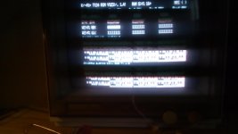
To give you an idea of what it will be. This is the one I built that accesses via the CPU socket, it was built on a generic prototype shield. Underneath the board is a mass of hand soldered wires and the pins to plug into the arduino. I didn't use a dip plug on the prototype because I was in a hurry and ordering one via mail was going to take too long, I made a simply adapter pcb and used pin strips. The pin strips are ok for prototyping because I replaced the cpu socket in my model1 with a ZIF socket but the pins are too large and damages a standard ic socket. The final production board will have 2 headers and require no wiring, just basic soldering skills.
20180615_140148.jpg

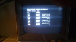
This is a board I threw together to do some static bus manipulation via the expansion edge, the same cable will be used for the production units expansion connector.
20180615_141426.jpg
 
Last edited:
I got bored tonight so I spent 90 minutes and put together a prototype shield for the expansion interface functionality. I decided to put it on a different shield because the rats nest of wires for one header is bad enough.
Hopefully I'll have time to begin writing the code changes needed to support it after the weekend.
20180615_230834.jpg20180615_230853.jpg
 
Last edited:
I managed to find a few hours last night to do some coding. I can read/write screen RAM, read ROM and read/write to the IO ports. My model 1 is still broken and I need to reinstall a 48k mod so I can test dram read/write works and then implement the changes to the refresh subroutine to support the new interface. So the good news in the schematic works as intended and most of the code is done.

Update: The refresh code now work and read/write to DRAM is also working. I put 48k RAM back into my model1 and it wasn't working due to a cut track I had missed from the old 48k mod I removed. The ICE in combination with a cheap logic analyzer off ebay made the process on finding that cut track unbelievably simple. I didn't know if my code in the ICE was bad or the RAM was actually bad (more problems in the model1 to track down yet). So I looked at signals on a single RAM chip, what I discovered was that writes to RAM work but reads were failing. I could actually see the data bit was being set low because could see a clear picture of the signals with no extraneous activity. On a read I could clearly see the data out line was either low or high depending on what I last wrote to that location, what was faulty was the read enable line was not activating to put the data on the bus due to the cut track.

Here is a capture from a single read from DRAM triggered on RAS going low with refresh disabled.
Untitled-1.jpg

I also added code to checksum the TRS-80 ROMS and fixed some bugs in the original code.
If anyone doesnt want to wait and wants to build one by hand, let me know and I'll send the code for the arduino.

Just fixed the DRAM fault in the model 1, everything now tests perfectly via the expansion connector. The final fault in the model 1 seems to be an intermittent fractured trace somewhere between the CPU and the address/data buffers, that cant be tested from the expansion connector so I'll need to wait on the parts to make a proper cable to plug into the CPU socket without damaging the socket. The count so far is 6 separate faults in the model one, so as frustrating as the repair has been it has been a excellent test of the ICE.
 
Last edited:
I decided to push ahead and layout the pcb myself, I completed that and ordered 20 prototype boards just now.
I should have some boards to test in a little over a week.

This is roughly what they will look like, the empty holes are for the pin strips to plug it into an Arduino Mega2560 and a push button switch.
Untitled-1.jpg
 
I've sent the KiCAd schematic to Glitch who has volunteered to layout the board, which shouldn't take long.

FWIW, I'm happy to help do board layouts/PCB design when needed as well. I have quite a bit of experience.
 
Back
Top