• Please review our updated Terms and Rules here

word alignment directive for Z280

Plasmo

Experienced Member
Joined
Aug 29, 2017
Messages
217
Location
New Mexico, USA
Z280 has a 16-bit wide data bus so data structures should be aligned to word boundary (even address) for optimal performance. Right now I look at the listing and reserve a byte when needed to adjust the data structures to word boundary. My question is how to find out the address of buffers automatically created by gencpm? and how to adjust them to word boundary?
 
I'm not sure about gencpm but I've run into this several times when assembling programs using M80. The following conditional works for me:

IFT $ MOD 2
DB 0 ; Force word alignment
ENDIF
 
I have used something similar. If your assembler supports MACROs, you can create a macro called EVEN and there is no need to comment the code as to what it does (apart from the macro itself of course).

I would replace the 'DB 0' with a 'NOP' so that the macro can be used with code (if that is a requirement to speed things up in a Z280).

Please explain in a little more detail your issues regarding GENCPM please?

Dave

Thank you for the tip on aligning to even address.

The issue with gencpm is that I'm using gencpm to allocate data buffer blocks and directory buffer blocks (dtabcb. dirbcb) automatically. How do I find out whether these buffers are on even address boundary and if they are not, how to adjust them?
 
I think you'd have to trace through the BIOS structures, starting with the drive table returned by BIOS function 22 "get drive table" (which is what GENCPM uses as well, although it does not execute the entry but expects the first instruction to be LXI H,drvtbl). You'll have to walk through those structures to locate the dtacb and dircb. Also, non-banked systems use a slightly different setup for the dtacb and dircb, so be aware of that. Probably need to have the System Guide handy for this, section 3.3 specifically.
 
I have to rethink this: Since cbios3 is assembled as relocatable, the address offset of assembled data structure is not meaningful until it is linked. I can declare the buffer name as public and find out its location in the symbol file, bios3.sym.

During the gencpm, a series of rather cryptic messages are displayed for dirbcb and dtabcb of each drive:

Share buffer(s) with which drive (A:) ?

Available space in 256 byte pages:
TPA = 00CDH


Is this a clue of where dirbcb & dtabcb will be placed?
 
Note, the BCBs are the structures that define/manage the buffers, not the buffers themselves. I guess that raises the question: are you trying to force all 16-bit loads/stores onto even memory addresses? or is this just about the I/O buffers?

For aligning at compile time, you can rely on the BIOS starting on a page boundary. So, you can leverage that knowledge to force buffer/structure alignment, in spite of the fact that REL files can be relocated to any byte address. The REL files are used to create an SPR (System Page Relocatable) which forces a page boundary.

The other way is to "allocate" the buffers (and possibly BCBs) at cold boot time. You have full control then, albeit at the cost of extra code. But for data buffers you'll have to put them in common memory (unless you support XMOVE) which will require allocation at compile time, or at least link time.
 
Ah, I see now. the value displayed during gencpm is a pointer to the actual buffer.

Z280 can handle word transfer to odd address boundary transparently but requires two data accesses. Only buffers contain large amount of data should to be on even boundary. For an example, the buffer that holds CF 512-byte sector data. Maybe there are other buffers like that, but I don't know.

Allocate the buffers manually is certainly a possibility. It seems manageable in non-banked version, but buffers seems pretty complex in banked version.

Another possibility is to turn on Z280's DMA hardware. According to the manual, there 4 DMA channels; they have 24-bit address and can directly access the physical 16 meg memory space regardless of the MMU configuration. With the DMA running, I probably care less about whether buffers are on even boundary or not. Another benefit of having DMA is simpler RAMdisk algorithm. Yep, it is time to turn on the DMA...
 
With the DMA running, I probably care less about whether buffers are on even boundary or not.

Double check with the docs... the DMA engine may also be affected by unaligned addresses. You'll also need to compute the physical address when setting up the transfer - not sure if that's a problem or not.

Regarding allocating buffers a boot time, I'm not sure it's really very complex in either case. You can hard-code your BIOS to a particular configuration, such as 2 buffers each for dtabcb and dirbcb, and then your cold boot routine just assigns addresses like 0100, 0300, 0500, ... for each of the buffers. All structures are in the BIOS, so you have direct access to them.
 
Can I offer a quick 'sanity check' here?

Why are you bothering too much about ultimate performance when you are running CPM?

I suspect that the innards of the BDOS are not optimised; and this is probably where you will loose performance on system calls.

It sounds an interesting project though!

Dave
 
Yep - written in PL/M. Not changed for the '80.

Was re-written in 'C' for the 68K and Z8K implementations.

Dave
 
DMA requires word transfer to be aligned on word boundary, so I do need to program the DMA to transfer data as byte. When power up, the MMU is transparently mapped, i.e. the 64K memory is mapped to the first 64K memory of the 16-meg DRAM. If I use DMA, I don't even need to turn on the MMU (for non-banked system). The RAM disk is located at high 8 megabyte memory so translation of track/sector to physical memory is pretty straight forward.

Far as 'sanity check' goes, I view performance improvement as 'low hanging fruits'--I'll go for it if it is easy. If it is hard, I'll try something else or not doing it at all. The trouble is I don't know whether it is easy until I've explored the various avenues. By then it may've became easy even though it was hard in the beginning. :p Anyway, I need to know DMA to work on banked CPM3, so might as well get it start.
 
DMA requires word transfer to be aligned on word boundary, so I do need to program the DMA to transfer data as byte.

Right, so it sounds like you take a performance penalty either way, if your buffer is not aligned. I'm looking towards the banked version, since that's where you want to go anyway (non-banked CP/M 3 isn't much to look at). In that case, you'll need to construct a physical address for the DMA address, based on what bank it is in. That may be trivial, but will depend on how you bank memory. If you throw away the top part of each bank, it is pretty straight-forward.
 
>>> BDOS3 is written in assembly.

You learn something every day...

>>> As far as 'sanity check' goes...

As I said, it all sounds a very interesting project! I am interested in the outcome as well for my own education - not that I will make much use of it in the near term - but I would like to get a Z280 going myself someday...

The last time I used a Z80 'in anger' was in a communications environment with two 250 kbps Z80 SIOs running HDLC protocol and an ETHERNET port. These units had Z80 DMA devices also. Although, in this application, it had a bespoke real-time operating system inside that I was bug fixing...

Dave
 
As I said, it all sounds a very interesting project! I am interested in the outcome as well for my own education - not that I will make much use of it in the near term - but I would like to get a Z280 going myself someday...

Dave

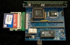
This is the Z280 SBC as it stands today. It is a simple design fitted easily in the inexpensive 10cm * 10cm 2-layer pc board. The two empty 32-pin sockets are for RAM and Flash during the early part of hardware development but are no longer needed. The RAM is replaced with the 16 meg DRAM and the flash is replaced with the compact flash. So there are room for peripherals like Ethernet and HDLC.

I "discovered" Z280 about 30 years late. The part is readily available from UTSource (China) and cheap ($3) with date code from 1992-1997. There are many negative comments about this processor mostly about it being buggy but I have not encountered any significant bugs. In fact, the only bug I know of is the internal refresh counter can't be turned off with value of 0x0.

I'll place my design and software in public domain the in retrobrewcomputers wiki. You are welcome to use them as you see fit.
 

Attachments

  • TinyZ280_RTC.jpg
    TinyZ280_RTC.jpg
    100.2 KB · Views: 1
Back
Top