I used 27C256. (in fact on all the eproms)
Cool, I'll try that.
I used 27C256. (in fact on all the eproms)
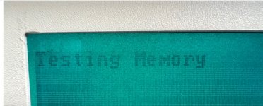
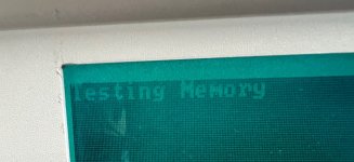
I got an immediate message saying that there was an error at 0000:0000 bit 0, so that seems to work.If you pull the memory card altogether and try to boot up, you should get an error at 0000 message. Try that, to see if at least that part of boot up is the same as others.
")
So, your character rom versus my character rom...
They are the same, except for one small detail...
(No change to the boot failure behavior, but it's cool to find it's just an inverted rom. I wonder - could we burn both onto a 27C512 (one rom in the lower half, the other rom in the upper half) and use a switch or jumper on pin 1 (A15) to choose between normal and inverted mode?
Normally, with an oscilloscope, yes. What you see will depend on the chip and the components connected to X1 and X2. An example is shown in posts #30 and #31 at [here].I assume that I should be able to pick up an sine wave (of whatever the crystal is rated for) between each of those pins and ground, correct?
You need to stop interchanging between "crystal" and "oscillator". It will lead to confusion. An "oscillator" is typically a self contained unit - 3 or more pins - feed it a DC voltage on one pin, and an oscillating signal (square, or sine, etc.) comes out another pin.I plan to pull the two caps and the oscillator off the board to test.
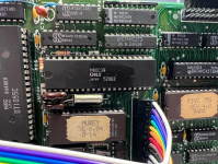
I looking at the Z-171 schematics at [here], the closest thing that I could find is the "KEYBOARD PROCESSOR", shown below, in which the main component between X1 and X2 is an inductor. Maybe an inductor was fitted in some Z-171's and something else in others.On the 80c39 ("Keyboard Controller" in the schematics) the two XTAL pins go to either side of a crystal oscillator, then both pins go to ground through big capacitors.

I looking at the Z-171 schematics at [here], the closest thing that I could find is the "KEYBOARD PROCESSOR", shown below, in which the main component between X1 and X2 is an inductor. Maybe an inductor was fitted in some Z-171's and something else in others.
View attachment 1265190
Normally, with an oscilloscope, yes. What you see will depend on the chip and the components connected to X1 and X2. An example is shown in posts #30 and #31 at [here].
You need to stop interchanging between "crystal" and "oscillator". It will lead to confusion. An "oscillator" is typically a self contained unit - 3 or more pins - feed it a DC voltage on one pin, and an oscillating signal (square, or sine, etc.) comes out another pin.
In the photo you posted, Y2 is a crystal. Hence my earlier statement of, "Maybe an inductor was fitted in some Z-171's and something else in others.'That is the chip. Y2 is an inductor? I thought it was a crystal oscillator...
At [here], there are photos showing inside a 'crystal'. It doesn't oscillate by itself. It is used as part of an oscillator circuit. It has no polarity.You are correct, I need to look closer - the concept is clearly not as simple as I had thought.
They are capacitors. Remove them and see what the measured capacitance is compared to what is printed on them.I have some reading to do on the thread you referenced. Specifically in how the two capacitors should read, ...
It is going to vary from circuit-to-circuit.... and what those two pins should look like.
However this inductor/crystal is the first inconsistency I have noted in the schematic compared to my board (while working through my troubleshooting) so it's still the best place to start. I'm considering redrawing the schematics in a modern piece of software, unless anyone knows of a better quality version out there? Some of the text is too blurry to read and I have to rely on following the traces and reading chip datasheets to figure out a lot of it.