• Please review our updated Terms and Rules here

(Another) Model 1 video problem

BartH

Experienced Member
Joined
Mar 11, 2015
Messages
72
Location
Netherlands
All,

I got this modified M1 and I tried to bring it back to life and remove some of the odd modifications such as an connector for an external keyboard. One modification is still in place which is a new character rom. The M1 boots but then shows two errors:
- many characters are replaced by a solid white block, strangely it overlaps the next character a bit. Video ram has already been tested and replaced.
- The return-key doesn't give a new-line: on the Memory Size prompt the cursor goes to the right instead of a few lines down.

Picture:
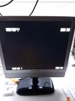
WhatsApp Image 2016-08-17 at 20.19.27.jpg

And a small video:

Anyone a clue?

Bart
 
Bart,
Your Model 1 has one of two sign on messages:

MEM SIZE?
4D 45 4D 20 53 49 5A 45

R/S L2 BASIC
52 2F 53 20 4C 32 20 42 41 53 49 43


MEMORY SIZE?
4D 45 4D 4F 52 59 20 53 49 5A 45

RADIO SHACK LEVEL II BASIC
52 41 44 49 4F 20 53 48 41 43 4B 20 4C 45 56 45 4C 20 49 49 20 42 41 53 49 43


You should know which one the messages is displayed on power up. This is determined by what code is in your ROMS (EPROMS).

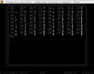
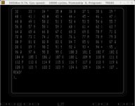
Instead of getting the standard ASCII characters, it appears you are getting a Graphics character.
Can you find out exactly what Graphics character is displayed from the attached file as your video
doesn't display it well enough to see. You can use the SHIFT then RIGHT ARROW to put your display
in 32 Character mode to make the graphics block larger on the monitor. Maybe it's a 0xBF (191) character?

http://www.kreativekorp.com/software/fonts/trs80.shtml

That value in HEX is the difference from the standard sign on message (in HEX) shown above.
Looks like a stuck data bit, causing the Graphics character versus the standard text.


Also, I'm interested in the NEW Character ROM. Where did you get it and can you upload a picture of it and
tell us more about it? Is it in EPROM or a Flash IC? How did you adapt it to the motherboard? What is the speed
in ns of your new Character Generator? More information is needed.

Are you using some kind of In Circuit Emulator (ICE)? What is the extra ribbon cable attached to the Motherboard?

Larry


M1-Graph.jpg

M1-Text.jpg
 
Last edited:
FWIW, based on your video, it appears you have the older "RADIO SHACK LEVEL II BASIC" ROM. It looks like I can see "RY" from "MEMORY SIZE" in the message.

Tom
 
I think Tom is right and the text is MEMORY SIZE, thus an older Rom. It's an older M1 with the two roms and Level II on a satellite board. The character generator is from unknown origin as I just recently bought the M1. It's on the other satellite board with the blue ribbon.
It's probably not the 191 character as I see a slight offset between the readable characters and the white blocks. Apart from that, the first E is not visible where the second is, so the character rom appears to work. The display memory has been tested with a Fluke 9010a and is 100% correct.
Apart from that, pressing Enter moves the cursor to the right instead of down. Very puzzling this all, I can't see of any logical explanation....

Bart

WhatsApp Image 2016-08-14 at 12.51.31.jpg
 
@BartH
?? would it be that the "Enter" Key is not being interpreted as an enter ?? as well but as a character that produces a 191 ??
I would also like to get a dump of the Character Gen Eprom, also what is Written on the Eprom ??
Thanks Ray
 
My first step would be to fit an original character generator in there to see if that changes anything. It's possjble the eprom doing the job currently may have bit rot...

Quite so, but where do I find a new character ROM? I won't be too happy to cannabilize a good M1......
 
Barth,
I sent you a PM previously and you didn't respond. Did you receive it?

Try this:
The address lines are outputs from the Z-80 used to specify memory locations. If any address line is not active (stuck on one state),
there will be 'garbage' (random characters) on the screen at boot. To check the address lines, remove the DIP Shunt at position Z3 and
power-up the system. MAKE SURE YOU NOTE THE DIRECTION IT WAS ORIENTED IN THE MOTHERBOARD. If the screen fills
with a pattern of “@9@9@9@9...”, then all the address lines A0 – A9 are good. The remaining address lines A10 – A15 can be checked
for activity with a scope or logic probe.

If the screen shows “@9@9” in some areas and garbage characters in others, in a repeating pattern, the defective address line can be
found easily. For example, if the pattern is alternately four characters of @9 and four of garbage, then address line A2 is stuck because
2^2=4. If the pattern is a full line of @9 (64 characters) followed by a full line of garbage, then address line A5 is stuck because 2^5=64.

If you suspect problems on an address line xx, you can easily build an address line tester from an old functional Z80 CPU. Then you can
chase each and every address line across the motherboard with an O'Scope or logic probe. (I prefer an O'Scope.


Any data line without activity will also cause garbage. Remove Z3 and look at the display. An inactive data line will often cause a pattern
on the screen like @1@1 or Y9Y9 and the bad bit can easily be found. Since the correct pattern is @9@9, the stuck bit can be
determined mathematically (similar to bad address lines above, subtracting the binary of @ or 9 from that of the character seen).
The most common cause of a stuck data line is a bad memory chip, the inputs of which are tied directly to the data lines.
Removing all memory chips and checking the pattern will identify whether the problem is RAM or some other chip.

You could also built a nice In Circuit Emulator (ICE) to help you debug it. Just takes an Arduino Mega 2560 and a Prototype board
with some headers and cable.


Larry
 
Last edited:
I'd be more inclined to think the problem is associated with the Video Ram Bit 7 that selects text or graphics, that is fiddling with the data bus.


If you remove the following IC's:
Z80 CPU Z40
ROMA Z33
ROMB Z34
RAM Z13..Z20

and still have the Video RAM (2102AN) installed at:
Z45-Z48 & Z61-Z63


What is on the Data bus will be on D0..D7 at Z75, Z76 & Z55 (74LS367)
with the Data either as an INPUT to or OUTPUT from the LS367 Buffers.
The DIR is selected from Z40 (Z80CPU) Pin 21 (ZRD* = LOW) via Z53 Pin 6.

Find out what is on the Data bus (D0..D7) with all the above IC's removed and in the RD state.

By pulling the Z80 RD Pin LOW at CPU Pin 21 you should get the Data (D0..D7) at the CPU Pins.

This same information is going to the IC's that decode the Text Bit Pattern OR the Graphics Pattern.
Maybe try swapping the Bit 7 Video RAM for the Bit 0 Video Ram.

If you follow the Output of the Video RAM (Z63) on Pin 12 to Z27 Pin 4, that gives one of the following
choices. Either (DLY BIT 7* = selects Z26 Pin 8 = TEXT MODE) or (DLY BIT 7 = selects Z26 Pin 6 = GRAPHIC MODE)
to allow Z10 to shift out the Text on Pin 13, or Z11 to shift out the Graphic on Pin 13.

I still think it's something fiddling with the Data Bus for Bit 7, because a couple of characters appear to be correct.

Does this make sense?


Larry


text-graph.jpg
 
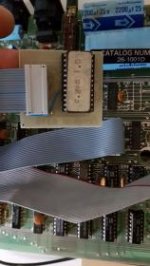
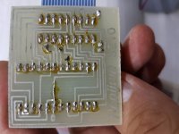
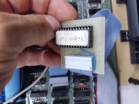
Ok, I got some progress! The character generator rom appears to be a 2716 and its contents have been dumped. The board is marked Nenijwa which is/was a Dutch company selling supplies and parts for the TRS-80 in the eighties. So the character ROM was a commercially available product, although the soldering and general tidiness of the board assumes a lot of hobby-work. Probably what is known in English as 'Cottage Industry'.


Link to my dropbox with schematics, pictures and the bin-file: Link


Pictures of the board:20160902_193715.jpg20160902_193750.jpg
 
BartH,
I've downloaded the .BIN & .PDF files. I've had a look at the .BIN with my HEXEDIT program and it doesn't look like what I'd expect.
But, I need to decode a character to see if it appears correct.

I'm curious why they didn't use RS1, RS2, & RS3, as A0, A1, & A2 on the 2716, because there are 8 Rows of Bits (2^3 = 8) for each character.
By having R1 tied to A9, RS2 tied to A8, and RS3 tied to A0, it's going to be confusing to decode, since all the rows for each character will
be spaced about in the file.

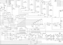
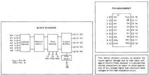
I've attached the info on the Original Character Generator, but I'll bet you have already seen it. Your socket is 100% correct.

The Original Character Generator put an address on {A0..A6} (2^7 = 128) for the address of a Character, and then read the 8 rows {RS1..RS3} (2^3 = 8) for {R0..R7}.


Larry


MCM6670-1.jpg
 
Last edited:
BartH,
I've succeeded in decoding the first character as an "@" and that matches one of my TRS-80 Model 1's Character Generator files.

But, after doing all the characters, they don't look to be in a proper order. So, I checked my address decode and I found an error.
So, I've updated the information below and I'm reworking the decoded characters.

Basically they have wired the addressing for each Characters ROW position for address X as:

Row 0 = Address X
Row 1 = Address X +200
Row 2 = Address X +100
Row 3 = Address X +300
Row 4 = Address X+4
Row 5 = Address X+4 +200
Row 6 = Address X+4 +100
Row 7 = Address X+4 +300
NEXT CHARACTER = Address X+4 +4

That gives all the ROWS in a scattered file.

Then the decoded ROW Data becomes:
Bit........ O2 O1 O6 O7 O5
Wired to D4 D3 D2 D1 D0


Which gives the character. So, If you read the EPROM correctly, and I think you did, it is working correctly.
Which means it should display correctly if something isn't setting the MSB switching in the Graphic Mode decode.


I'll send you my updated Spreadsheet in the morning with details of what I did. (during FREE Upload Time).

Larry
 
Last edited:
Back
Top