Upcoming Events:
| VCF West | Aug 01 - 02 2025, | CHM, Mountain View, CA |
| VCF Midwest | Sep 13 - 14 2025, | Schaumburg, IL |
| VCF Montreal | Jan 24 - 25, 2026, | RMC Saint Jean, Montreal, Canada |
| VCF SoCal | Feb 14 - 15, 2026, | Hotel Fera, Orange CA |
| VCF Southwest | May 29 - 31, 2026, | Westin Dallas Fort Worth Airport |
| VCF Southeast | June, 2026 | Atlanta, GA |
-
Please review our updated Terms and Rules here
You are using an out of date browser. It may not display this or other websites correctly.
You should upgrade or use an alternative browser.
You should upgrade or use an alternative browser.
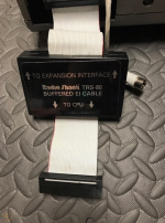
Buffered E.I. cable
- Thread starter GK2001
- Start date
Eudimorphodon
Veteran Member
I have one with a cracked open case that I’ve been meaning to probe out, I guess I should do that. It has been on my list to build a replacement PCB that has 32k SRAM chip and ties A15 low to override the EI memory because I’ve kinda lost patience with the whole DIN plug mess.
NeXT
Veteran Member
There's pictures floating of the NewBuff which was a replica of the buffered EI cable but it seems the site that lists it is currently down. I think the photos still work though.


Eudimorphodon
Veteran Member
I just popped the lid off my original and did a little probing. Looks to me like, no, they're not, the D* signals pass straight through from one side to the other. Looks like the three '244s are entirely just addresses and control signals.
That's what I figured. If there was a bi-directional buffer such as a 74LS245 to handle the data lines, it would need an enable line derived from the address decoding inside the E.I. unit to prevent read contentions with the keyboard unit.
Dawsoca
Experienced Member
I just checked and Ian's site is working, you can find the NewBuff on this page: http://members.iinet.net.au/~ianmav/trs80/newstuff.htmThere's pictures floating of the NewBuff which was a replica of the buffered EI cable but it seems the site that lists it is currently down. I think the photos still work though.

oktology
Experienced Member
You don’t happen to have any of his other schematics, do you? His website is gone and archive.org doesn’t seem to have archived any of the downloads.This is an old schematic from Pascal Holdry who did a lot of amazing work in recreating the TRS-80 hardware.
> Charles
hornbetw
Experienced Member
Ian's site is at http://www.trs-80.com.au/trs80/index.htm

