I'm seeing just 6x 27HC641 8kx8 45nS PROMs on the T1002 module, which does indeed correspond to a 48-bit uWord :->.
I think you're thinking of the HSC50 L0107 which has 12 prominent PROMS (apparently AMD but I can't find a photo with enough resolution to make out the PN).
Hi again. As for the number of PROMs, I was talking about the UDA50 controller, which has 6X2, the same as the L0107 in the HSC50. Both were developed early on (about 1980-ish). All the later products (starting with RC25, then KDA50, then KDB50) had just 6 chips. The next controller, the KDM70, didn't use the 2901 architecture at all - I don't remember much else about it, except that it was mostly surface-mount chips, which was a new-ish thing for us.
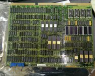
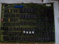
Don't you mean the K.pli (L0107) here? I've attached a photo of what I believe to be the K.sdi (L0108) module; also a (dark!) photo of a K.sdi (L0107) that I found online.
Yes, you're right! The "K.SDI" name should have been a hint (SDI is the storage interface, not the processor).
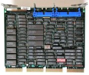
Trivia regarding the L0108 (similar for the UDA50's SDI module): IIRC, the 3 bigger chips near the middle are what we called "SERDES" (serializer/deserializer, a fast UART-type device). The guys to the right with the black heat sinks are "ENDEC" (encoder/decoder, converted the serial bit stream to the encoding used by SDI, sorta like the 8/10b code used in FibreChannel). The hybrids in the upper-right are the electrical interface to SDI.
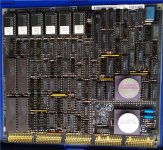
Meanwhile, attached is a pic of the KDA50 and KDB50 controllers. I built the Manufacturing Functional Tester for those also.
The earlier testers included a WCS (writeable control-store) which "replaced" the PROMs via the bed-of-nails vacuum fixture, allowing me to run my custom diagnostic code during the test without physically removing the PROMs.
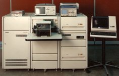
Also attached is an 'official' pic of the KDB50 tester. Unlike the earlier testers, it was no longer practical to use a bed-of-nails fixture (mostly because of the BI bus, IIRC), so I used a BI backplane, a known-good SDI module, and a complete HSC50 cab. So very little custom HW in the tester; mostly just some SW.
Pete
")