• Please review our updated Terms and Rules here

Building my own ZX80

That was the Sinclair way - make it as cheap as possible!

But, lots of people could afford a ZX80/ZX81 (and the later Spectrum) and (as you say) they served a useful purpose in education.

It would be an interesting 'thought experiment' to work out what Sinclair would have produced if he had got the Contract to build the BBC Computer though... Just to pass the time!

Dave

Well, that was the Spectrum wasn't it. I don't know if he would have done it any differently, given that it was what he provided as his "entry"...

The real thought experiment that gets me thinking is what would the Loki have looked like? I'm about halfway through building one, and seeing how minimal I can get it, and so far, a 512x192 video display requires only 2 PAL chips to do all of the raster timing, and I managed to eliminate multiplexers by sharing the bus. Based on what he was likely to buy at the time, It would have performed at access speed of 210ns, which would allow for a Spectrum running at 14MHz with a CMOS chip overclocked. I'm just working on assembling parts for a prototype at the moment. It's not that easy to do, using only tech from 1985.

That wasn't supposed to just keep up with modern machines, but perform graphics like an Amiga, Maths like an IBM, Sound like an Atari ST and still cost under GBP200... which was around USD$400 back then. It would have been truly amazing.
 
>>> Well, that was the Spectrum wasn't it

True...

I have seen your posts about the Loki...

Dave

I am definitely in the minority of people who believe it was possible. :)

But the zx80, zx81 and zx82 make me believe he would have succeeded. His specs are not as unimaginable as many would believe.

Everytime I look at the zx80, I'm reminded of how clever it was - and in it's era, it really was incredible.

At the time though, I didn't understand why it couldn't display and process basic at the same time. the ZX80 didn't have slow mode like the zx81, though it was upgradeable.

Personally, I loved the style of the case. There's something about a zx80 that deeply resonates with my feelings about what a computer should look like.
 
Your troubleshooting should take into consideration how the zx80 works.

First, you want to make sure that the z80 is executing all the code in the ROM correctly, and that ROM and RAM and being selected and providing a signal. As was mentioned, making sure all of the lines are connected and none are shorted is critical, but doesn't take that long when you sit down with a multimeter to actually do it. Debugging a new system is a bit different as an approach to repairing an old system that used to work. It doesn't take long with a multimeter and continuity check to make sure all the address and data lines from the CPU make it to the memory. A z80 will work with just memory, select arbitration logic and the CPU with a valid clock. You can troubleshoot the video once you know the computer core itself is working.

Some steps that may help.

1) Check all address and data lines make it from the z80 to the ROM and RAM. Check between them (eg, A1 to all other z80 pins ) to ensure no fundamental shorts. - You can also do this on the ROM and RAM select lines to make sure there's no post-logic shorts. It takes about 20 minutes for a board of the size you're making. Note that the address lines to the ROM are interrupted by the 74ls157 multiplexers, so you will have to check from the z80 to the MUX, and from the MUX to the ROM. The RAM should be direct via resistors. The resistors (1K) will likely affect continuity, so check from the resistors to the data lines and from the resitors to the z80.

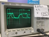
2) Check that the select logic for the ROM and RAM is working OK and both are being selected.

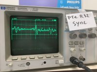
3) Check the relevant address lines are being used - ie, the z80 is clocking.

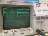
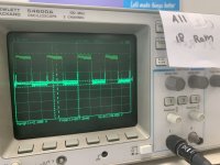
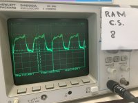
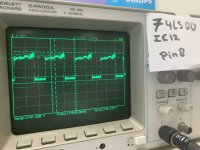
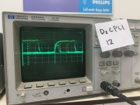
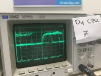
4) Check the decode logic with a dual trace if possible, or get a cheap ($10ish) 8 pin logic probe to check the ROM and RAM are being selected correctly. You can check the z80 timing waveforms in the manuals to see what they should look like.

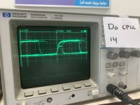
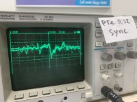
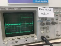
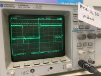
5) Once you are confident that the z80 is running, there is a circuit to feed the z80 NOPs while the address lines increment so that the video can be generated which you can check - it's via Open Collector outputs that just pull the bus low when it reads an instruction. Other stuff will happen when this occurs, such as the multiplexers being activated to read the character ROM from the RAM data bus. Also there should be data latching into and clocking out of the shift register. You should be able to see the timing around this as approaching 64uS per line.

6) Review some pages on how the zx80 works to better understand what you're looking for.
Eg: http://blog.tynemouthsoftware.co.uk/2023/10/how-the-zx80-generates-video.html
Thanks for all the steps and the website! I will take some time to read it and use your steps Friday. I’m very happy that you all take the effort to help me. This is how you learn stuff! :)
 
So, today I spend some time to work on the ZX 80. I started with checking the address and data lines for shorts and if they are connected how they supposed to be connected. There were some very small shorts (I added some pictures). But the power usage is now around 390/400mA, that seems better!

I also probed at the “chip select” from the ROM and RAM (see pictures). I’m not sure which one the “output enable” is, I have two ROMS, a programmed 2732 (with the mods according to http://searle.x10host.com/zx80/zx80.html )

And a Rom which I have from eBay, the person said that it worked and was “original”. I have no picture yet, but I can’t find anything about the number written down at the ROM, I will provide a picture later. At the website from Grand, different ROMs are compared.

Besides that, I have taken a look at some data and address busses. The signals at the databussen are a bit “trashy” (I do not know how to name it properly ;) ).

The address bus signals are looking more straight.

I also probed on the chip select from the RAM, but it looks a bit weird. I have a picture from pin 8 of the TTL that looks a bit more like an high/low signal. After the resistor, it’s more round shaped. I don’t know how bad it is if the tel signals are not very nice shaped.

Dave, I also proved before the resistors for sync and video (see pictures, noted as “pre R30/32”.

If I prove the combined signal before entering the RF modulator, but after the resistors, I see signal changing if I short a keyboard “pad”. So something is hapening!


Well, I will add the pictures. Again with the pins noted on paper. If anything is not clear, please let me know.

Step by step I’m getting there!
 

Attachments

  • IMG_8080.jpeg
    IMG_8080.jpeg
    1 MB · Views: 9
  • IMG_8081.jpeg
    IMG_8081.jpeg
    646.2 KB · Views: 9
  • IMG_8082.jpeg
    IMG_8082.jpeg
    898.8 KB · Views: 8
  • IMG_8087.jpeg
    IMG_8087.jpeg
    2 MB · Views: 8
  • IMG_8085.jpeg
    IMG_8085.jpeg
    2 MB · Views: 7
  • IMG_8089.jpeg
    IMG_8089.jpeg
    2.1 MB · Views: 6
  • IMG_8092.jpeg
    IMG_8092.jpeg
    2.1 MB · Views: 9
More pictures:
Please not that some pictures are from the same signal (video signals), but with different timebase and or voltage then the rest of the measurements.
 

Attachments

  • IMG_8093.jpeg
    IMG_8093.jpeg
    1.9 MB · Views: 4
  • IMG_8094.jpeg
    IMG_8094.jpeg
    2.2 MB · Views: 5
  • IMG_8095.jpeg
    IMG_8095.jpeg
    1.9 MB · Views: 5
  • IMG_8096.jpeg
    IMG_8096.jpeg
    2 MB · Views: 6
  • IMG_8097.jpeg
    IMG_8097.jpeg
    1.9 MB · Views: 5
  • IMG_8102.jpeg
    IMG_8102.jpeg
    2 MB · Views: 5
  • IMG_8103.jpeg
    IMG_8103.jpeg
    2 MB · Views: 5
  • IMG_8100.jpeg
    IMG_8100.jpeg
    2 MB · Views: 5
Making sure every single trace works and is not shorted is, unfortunately, the first step to troubleshoot such a PCB. Having a detailed knowledge of what every line should/must do is critical as a second, otherwise you won't know if it's working.

Square waves look pretty, but in the real world, a resitor and capacitor ( or just speed in faster cases ) will give you the RC charge shape like you're showing. That's fine. Once the signal crosses a threadhold ( let's assume around 50% unless they are scmidt triggers ) then the signal has changed. It can be harder if you're not sure where the edge should be, but that shouldn't be an issue for a design that is proven like this. I've seen it cause problems in working computers, but that should not be the case here.

A logic analyser would be the only easy way out here. Attach it to pins and see what is happening. Also an eprom reader would help you make sure the ROM is doing what it is supposed to do. Also, there's the possibility that a chip is faulty, but I'd still guess that once you have all the traces connected without shorts, there's a really good chance it will start working.

I used to etch my own PCBs and it can be a slow process to do that. I still make my own PCBs but now I machine them. It's a nicer way to do it and after machining, I use a microscope to look for issues. that's also an idea since it looks like you have a microscope.

Can you briefly list what equipment and tools you have? The oscilloscope and microscope are obvious, and I assume a multimeter with a fast continuity, but do you have a logic analyzer? And how many bits? This will help you make sure information is doing what you expect it to.

I don't know how they troubleshot the zx80 in the 1980s. I suspect many never got completed.
 
The VIDEO signal looks healthy.

The SYNC signal not.

These "Pre Rnn" signals should be logic levels. The VIDEO signal is, but the SYNC signal is not.

If I understand your oscilloscope display correctly, the settings are Y = 200 mV/div and X = 20 ns/div. This signal is way too low (in terms of the Y voltage) and the oscilloscope timebase is much too fast to see the H and V components of the synchronising signal.

Look up what a video signal SHOULD look like (especially the SYNCHRONISING component timing) - bearing in mind that we are looking at LOGIC LEVELS, with the composite signal itself being produced after the resistors.

I suspect what you are looking at with your oscilloscope on the SYNC signal is noise.

In my mind, the H SYNCH is round about 64 us; with the V SYNCH round about 16-20 ms. Your oscilloscope timebase needs to be set accordingly.

Dave
 
Thank you both for your reactions.
I had some other stuff on my mind this weekend. So I will make this week an overview of the devices I have available to do troubleshooting. I plugged it in on my television, just out of curiosity, and indeed I get no image. You can see that the tv senses something. But it is only snow.

So I will take a look at shorts etc. At the sync part of the PCB and TTL’s. There are digital tektronic scopes available in the nearby room at school, but most of the times, they have labs there. So I will try to do some measurements with those for a more clear picture.

Thank you for the explanation of the not straight lines because of capacitance and resistance combinations. That makes things more clear!
 
TTL logic is good for pulling signals LOW. When the TTL output goes HIGH, there is an effective internal resistor pulling the signal HIGH, this generally makes the output of a TTL gate 'horrid' looking, pretty much as you have...

Bus buffers (on the other hand) have active logic to pull the signal both HIGH and LOW, so the signal outputs are much more 'square'.

However, to save costs, guess what - you won't see bus buffers anywhere...

Dave
Ah okay! Thanks for the information. Now I know why I get the “horrid” looking stuff. I like learning :)

I’m sorry that I post a reaction so late. I have exams soon. I’m a bit busy with that now. But when I continue with with the ZX80, I will post information according to the project or questions for sure. I hope that’s okay.

Regards, Ben
 
From the datasheet the NEC D780C-1 is a 4 MHz part. I was wondering whether it was a 2 MHz part running at a higher frequency, but that is not the case.
In case it's not well known here, it's worth mentioning that this is a super-common part used in literally millions of units of home computers, just mostly in Japan. I reckon that the NEC parts are not so likely to be remarked, simply because they're not as well known; if you're going to remark parts you might as well go for the original and (outside of Japan) much more recognised Zilog name and part number.
 
In case it's not well known here, it's worth mentioning that this is a super-common part used in literally millions of units of home computers, just mostly in Japan. I reckon that the NEC parts are not so likely to be remarked, simply because they're not as well known; if you're going to remark parts you might as well go for the original and (outside of Japan) much more recognised Zilog name and part number.

I think many rebadged z80's could be literally anything with 40 pins. I've got a few brand-new "z80s" that have entire chunks missing from the case - on the underside of course where they didn't realize. They could be anything.

I've bought un-remarked CPUs too, and they appear to be legit, but often they have a fault - eg, Faulty data or address line - I suspect when they are trying to remark z80s, these failed testing and so were not worth remarking.

The chip resellers probably have lists of which chips are compatible, and keep a mixed bag of them and then remark them with whichever part you order so they all come out looking the same, unless you turn them over and note briefly that all were a part of the same batch, but the underside markings and patterns are completely different chip to chip :(

I have some Toshiba z80 remarks on my desk at the moment. All the same batch, yet different case materials and die marks.

Now I don't trust any z80 except the ones I have tested and work.
 
Back
Top