- VCF South West - June 14 - 16, Davidson-Gundy Alumni Center at University of Texas at Dallas
- VCF West - Aug 2 - 3, Computer History Museum, Mountain View, CA
- VCF Midwest - Sept 7 - 8 2024, Schaumburg, IL
- VCF SoCal - Mid February 2025, Location TBD, Southern CA
- VCF East - April 2025, Infoage Museum, Wall NJ
-
Please review our updated Terms and Rules here
You are using an out of date browser. It may not display this or other websites correctly.
You should upgrade or use an alternative browser.
You should upgrade or use an alternative browser.
CBM PET 710 WITH BASIC PROBLEMS
- Thread starter Desperado
- Start date
daver2
10k Member
Try changing the oscilloscope synchronising onto the channel used for the address line instead of the NOP EPROM pin 22.
And adjust the oscilloscope timebase...
Dave
And adjust the oscilloscope timebase...
Dave
daver2
10k Member
Let's assume first that the problem is the person taking the measurements shall we?I suspect that Nop Eprom it's not doing its job..
Dave
Desperado
Veteran Member
- Joined
- Nov 25, 2017
- Messages
- 6,827
do I have to reverse the two channels?Try changing the oscilloscope synchronising onto the channel used for the address line instead of the NOP EPROM pin 22.
And adjust the oscilloscope timebase...
Dave
daver2
10k Member
We don't want the timebase to be full scale. That is the FAST end. We want to SLOW it down.
I am not sure what I am actually looking at on your last photograph.
Dave
I am not sure what I am actually looking at on your last photograph.
Dave
daver2
10k Member
Let's explain a little bit more...
The CPU (if it has a signal on pin 3 - SYNC) is fetching and executing instructions. We don't know where from yet...
The CPU should be outputting the address on the address pins of the CPU (A0 to A15) and the memory mapping register pins (P0 to P3).
With the oscilloscope set to single channel (and triggering on that channel) you should see activity on a subset of (and maybe not all of) A0 to A15 and P0 to P3 ON THE CPU.
You will have to adjust the oscilloscope timebase to see anything - and (even then) (depending upon WHAT the CPU is executing) you may not be able to get a stable oscilloscope trace. This is just life...
The CPU address bus (A0 to A15) is buffered by U19 and U18. In theory, what appears on the CPU address bus (A0 to A15) should appear on the input to (and output from) the address buffers. The address buffer outputs go to the ROM/EPROMs.
Likewise, the CPU P0 to P3 signals are buffered by U58 and then disappear off to more logic.
Now, here is the issue, the address buffers (U19 and U18) are controlled by a signal on pin 19 such that they can be enabled and disabled. So, if they are disabled, the CPU address lines still go TO U19 and U18 - but they may NOT appear on the output side (and hence on the pins of the ROM/EPROMs).
Look at the schematic https://www.zimmers.net/anonftp/pub/cbm/schematics/computers/b/8256059-01.gif and does this make sense?
Dave
daver2
10k Member
If the address buffers (U19 and U18) are enabled, the CPU address bus should appear on A0 to A12 of the ROM/EPROM devices.
If we see pin 22 going LOW on the EPROM - then the EPROM is being accessed AND the EPROM data is being output onto the data bus.
Look at schematic https://www.zimmers.net/anonftp/pub/cbm/schematics/computers/b/8256059-06.gif. Can you see that?
Dave
If we see pin 22 going LOW on the EPROM - then the EPROM is being accessed AND the EPROM data is being output onto the data bus.
Look at schematic https://www.zimmers.net/anonftp/pub/cbm/schematics/computers/b/8256059-06.gif. Can you see that?
Dave
daver2
10k Member
There is no point unless we know that the address bus is working.
How do we know what device is writing to the data bus (if anything is)?
We have no idea whether it is our EPROM or not...
Dave
How do we know what device is writing to the data bus (if anything is)?
We have no idea whether it is our EPROM or not...
Dave
daver2
10k Member
Use one probe of the oscilloscope, with the trigger set for that probe and adjust the timebase from slow to fast until something sensible appears - that is swinging from 0V to +5V.
See if you can use the trigger level to get a stable display.
If A7 is not oscillating, try A6, or A5...
Dave
See if you can use the trigger level to get a stable display.
If A7 is not oscillating, try A6, or A5...
Dave
Eudimorphodon
Veteran Member
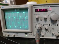
If i pur trigger channel also on pin 22 i have this..
I lost track, what two pins are seeing in this picture? (top trace is pin X, bottom trace pin Y, trigger is on [X or Y]?) And to be clear, this is when you're seeing sync signals coming out of the CPU?
Eudimorphodon
Veteran Member
We have no idea whether it is our EPROM or not...
In that earlier round where we were measuring the state of the data pins when the address bus appeared to be wedged at FFFF the byte the EPROM was asserting on the bus was an E0, which unless something changed with the file I attached to the forum *is* the data byte you'd expect it to be outputting for that address. If that was being measured incorrectly it seems like an incredible coincidence.
The EPROM feels like it's probably fine to me, and If it passes a verify test in the programmer it seems like it takes a lot of special pleading to blame the EPROM itself. The old PETs don't have a buffer between the ROMs and the CPU, which makes it a little easier to have confidence that the CPU is actually no-matter-what recieving what's coming out of any ROM you stick in a socket, but that previous fiddling with the data lines showed the same E0 on both sides of the buffer.
Desperado
Veteran Member
- Joined
- Nov 25, 2017
- Messages
- 6,827
Trigger is Y Eudi...I lost track, what two pins are seeing in this picture? (top trace is pin X, bottom trace pin Y, trigger is on [X or Y]?) And to be clear, this is when you're seeing sync signals coming out of the CPU?
Eudimorphodon
Veteran Member
Trigger is Y Eudi...
But what pin is X and what is Y??? (And is X the upper or lower trace?)
Desperado
Veteran Member
- Joined
- Nov 25, 2017
- Messages
- 6,827
I can't see any waveform also if slow down timebase...Use one probe of the oscilloscope, with the trigger set for that probe and adjust the timebase from slow to fast until something sensible appears - that is swinging from 0V to +5V.
See if you can use the trigger level to get a stable display.
If A7 is not oscillating, try A6, or A5...
Dave
