• Please review our updated Terms and Rules here

Circuit Design for "invisible" RAM sharing with a Z80 CPU?

Eudimorphodon

Veteran Member
Joined
May 9, 2011
Messages
7,074
Location
Upper Triassic
Been mulling over some ideas to resurrect a stalled "homebrew computer" project lately, and among the ideas I'm considering is changing horses in midstream to making a sorta-TRS-80 compatible instead of a sorta-PET compatible. (Mainly because the "market", so to speak, for Commodore respins seems kind of saturated right now.) This means switching to the Z80 CPU from the 6502, obviously. As it was my project had gotten far enough to at least demo sharing the same memory (ROM and RAM) between the memory-mapped video generation system and the CPU itself; this is easy on the 6502 because it has that property where the CPU reliably only ever hits the bus on one phase of the clock, allowing you to do whatever you want with the opposite phase. However...

Unfortunately the Z80 isn't polite like this. For some bizarre reason according to the docs I've found the Z80 qualifies memory reads on the rising edge of a clock cycle when it's doing instruction fetches:
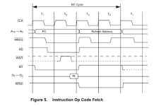
z80-instruction-cycle.png
But on non-instruction reads and writes it qualifies on the falling edge?:
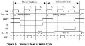
z80-read-write.png
So clearly a simple rule like "video can have the RAM on high phases" isn't going to do the job here. If I kept video memory separate from CPU RAM then the "simple" solutions are to either let the CPU always win (and deal with screen snow) or implement a wait state generator. (Which I'm a little fuzzy on but can probably find some resources somewhere.) But I'm curious what, if any, solutions people have seen/implemented in real-world designs to manage this?

FWIW, here's the "best" idea I can come up with, and I suspect it's not that great. Long and short of it: Z80 clock is a fraction of the dot clock never higher than half. For every phase of the Z80's clock cycle the video memory gets a full tick (or more), and the multiplexer will give the bus to the video memory for the earliest fraction of the Z80's tick. This results in continuous access windows for video memory that the Z80 isn't even going to know/care are stolen from it as long as the memory devices are fast enough to react to the address bus changes in a timely manner. Here's a genuinely terrible GIMP'ed timing chart I threw together to demonstrate the concept, the video access windows are in pink:
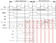
z80-interleave.png
(The fragment of chart under the VCLK line is T1/T2 from the instruction fetch chart.)

The big issue I see with this is the RAM and the multiplexing circuitry need to be lightning fast, since in this example I'm asking it to do the full access cycle on only half the pixel clock. That's going to be, what, 62.5ns for an 8mhz pixel clock? That makes the 55ns SRAM I'm using just barely fast enough for that, and realistically I need a pixel clock more like 12mhz. So... now this reads like an idea that *might* work if I used something completely supercharged like 20ns cache memory for VRAM, but it's not practical to use that for all the RAM in the system. Feh. Just talked myself out of that.

A variation of this idea is just choke down that the Z-80 effectively can't run faster than 1/4 of the pixel clock. The result is essentially the above but it divides access on full clock ticks instead of half ticks. (So imagine VCLK in that bad diagram being paced twice as fast, with two up/down transitions per T-clock phase instead of one.) Are there any deal breakers with this? If I were trying to emulate, say, a TRS-80 Model I I could use a 14mhz pixel clock (with 8 bit wide characters instead of six); a divide by 8 would give me 1.75mhz, which is pretty close to the original 1.77, and a /4 would be 3.5mhz, a decent speed bump. (A 14.7456 crystal is also a widely available option; that'd be a CPU of 1.8432 mhz, also close to the real thing, and would also offer a convenient clock for a UART...)

... Digging around it looks like the ULA in the Sinclair Spectrum does something kind of like this?(????) Except in the Sinclair's case it only holds the clock cycle long if video accesses are actually happening, otherwise everything proceeds at full speed. I'd rather avoid having the CPU run faster in the blanking area (except possibly as a select-able option) for compatibility reasons; the TRS-80 is chock full of software timing loops.

I guess I have another vague and probably bad idea about deferring video accesses to the opposite CPU clock phase if the M1 line is set when a video read is supposed to happen. IE, interleave the clock so video has the RAM on the low phases of the CPU clock, which should be compatible with normal read/writes if I'm reading the charts right, but if M1 and RD are set when the video read wants to happen it gets deferred until the next low cycle. If the output pixels for the shift register were "cached" in a latch then it'd probably be possible to get away with this and get the max CPU speed back up to pixel clock/2? Maybe?

Or maybe I should just use separate VRAM and system RAM. Just curious if this was actually doable.
 
If you're only going to be writing to video memory during vblank anyway, could you put the video memory in the IO space? CPU can fiddle with it during vblank, otherwise the RAM is owned by the video circuit? You'd just have to gate it off the bus while the video circuit was reading it.
 
If you're only going to be writing to video memory during vblank anyway, could you put the video memory in the IO space? CPU can fiddle with it during vblank, otherwise the RAM is owned by the video circuit? You'd just have to gate it off the bus while the video circuit was reading it.

I want memory mapped video (for speed and also at least partial TRS-80 compatibility), so I’m all in on having to have some kind of contention management even if I use separate RAM chips for CPU and video memory. A weakness of the TRS-80 architecture in particular is unlike the original Commodore PET (which suffered similar snow as the Model I if you wrote to the screen during the non-blank area) they didn’t even implement a way to *know* if you’re in vblank to avoid snow in software. (The PET has a blanking interrupt.)

With separate RAM life does get far easier, of course; the Model III uses a wait state generator, and that’s… fine. I was just hoping that maybe a Unified Memory Architecture might be doable because my video hardware supports both setting the character/framebuffer to arbitrary addresses (IE, multiple graphics pages and scrolling) and fetching character glyphs (“tiles”) from RAM as well. If I can use one big pool of RAM for everything instead of splitting it the flexibility factor is pretty compelling.
 
I would implement a "shadow RAM" for video. The Z80 reads and writes to normal system RAM. The video RAM is basically Write only.
Write to video address space writes to system RAM and you latch the address and data to clock that into video RAM using the character clock.
A read from video address space returns the data from the system RAM. Video RAM is never read by the Z80.
There is enough non access cycles to insure the video logic has time to finish before another write cycle can occur.
For example a LD instruction that writes to video memory will be followed by an instruction fetch.
A LDIR will always have T states that don't access memory between writes.

This was never used in vintage systems. RAM cost a lot. Now not so much.

joe
 
I would implement a "shadow RAM" for video. The Z80 reads and writes to normal system RAM. The video RAM is basically Write only.

I did think of that idea, actually, and it’s not a bad one. The main reason I’m kind of cool on it is, yeah, it means doubling up the RAM and it also means I need those latches and the associated state machine logic, but… I need to multiplex the address lines anyway and if video RAM is write only I guess it doesn’t actually need to increase the count much, it just means three ‘573’s instead of the ‘245 and whatever multiplexer parts I‘d otherwise use. And most of my logic is in GALs so the paced write state machine should be easy enough.

I’ll think on it. The other minor gotcha is with this plan I can’t share a single ROM between the CPU and video as well, but the flash ROM chips I’m using are dirt cheap so it’s just the PCB board space.
 
Okay, stupid question. Have you hung a logic analyzer on the subject Z80 system and verified the timings? Errata do exist, you know. :) I'd be more inclined to believe what I see with my own eyes, not something that a tech writer did decades ago.
 
Okay, stupid question. Have you hung a logic analyzer on the subject Z80 system and verified the timings? Errata do exist, you know. :) I'd be more inclined to believe what I see with my own eyes, not something that a tech writer did decades ago.

Hah! Alas I'm not beyond the brainstorming stage here, although I do at least potentially have the parts on hand to breadboard it. (This is for a "new" Z80 system from scratch, not an existing one.) At the moment I've been trying to dig up as much info as I can about Z-80 systems that did do unified memory architectures for ideas and technical details about how they managed it, but there is that issue of this architecture being pretty rare compared to 6502-based shared memory systems. (Hey... just remembered the Amstrad CPC series was another example...)

I found this old newsgroup article where a guy claims to have found a method for de-snowing Heathkit H19 terminals by multiplexing addresses on the low side of a CPU clock tick for video, high side for CPU, and it supposedly worked... but it came with the limitation that it was then impossible to run code from video memory because this wrecks being able to do an instruction fetch. (Which would follow if they didn't make an exception for the CPU being in the M1 state.) This suggest the manual is correct at least about the timing of non-instruction fetch read/writes, IE, they always commit on the falling edge of the clock, so I don't really have a reason to doubt the opposite it true for an instruction fetch. But... who knows if this recollection was accurate. It definitely wouldn't hurt for me to at least try sticking a logic analyzer on it to check, assuming the ancient Saleae Logic unit I have lying around is up to the task. (I might have to run the Z80 pretty slowly, I think the Saleae unit maxes at 20mhz sampling on a single channel and goes down as you add more.)

In reading this stuff I've run across a really confusing thing in the docs about the ZX Spectrum's clock-stretching state machine: the docs often refer to specific T-state numbers (table example here) and occasionally some authors make it read like/claim that its behavior is different depending on which T-state the CPU is in. If there's a Spectrum Wizard out there could you explain this in more detail? Because I have no idea how you'd ever determine what T-state the CPU is in with much reliability. I mean... it looks like technically you could with either an interrupt or a busresq get it started over again on T1 for the "response" machine cycle, but with instruction cycles taking 4 clocks and memory read/writes taking 3 how in the world would you continue pacing that? The M1 line is hanging loose in the Spectrum schematics, not connected to anything, so I can't even see how you'd *know* if a given cycle was an instruction fetch or read cycle. (I mean, I guess you could figure it out based on the length of the RD/MREQ pulse, but that's really getting out there.)

My best interpretation is that these numbers are just referring to a counter of ticks for each video frame that is reset when the vertical refresh interrupt is fired and the ULA *doesn't* actually have the capability to know how its current T-state aligns to the Z80's machine cycle states, but it's, like, totally unclear. Probably just a rathole worth avoiding.
 
Why not do your video refresh through DMA? That's the way we did it on the 8085.

After all, this is the 21st century--the age of "if it doesn't work, throw more silicon at it". :)
 
Last edited:
Why not do your video refresh through DMA? That's the way we did it on the 8085.

Was that using something like an Intel 8275 behind a 8257 or similar?

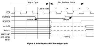
Alas I don't think that's really what I'm looking for here. So far as I can tell this sort of solution depends on being able/willing to halt the CPU during the active line area because you're essentially doing a bulk transfer between system RAM and the CRT controller clocked at the character output rate. (IE, around 2mhz for an 80 column screen.) What I'm looking for/need is a way to interleave CPU and video access with clock stretching or whatever so the CPU execution speed isn't affected (or is only minimally so) during the active area. The Z80 manual says the latency between asserting BUSREQ and the CPU actually granting access to the bus is "the end of the current machine cycle", and worse case that's four ticks (and completely unpredictable) so I guess I don't see how you're going to be able to interleave requests during this period. (The DMA controller is going to have just the same problem as the video hardware with contention.)

... If the BUSREQ signal is active, the CPU sets its address, data, and tristate control signals to the high-impedance state with the rising edge of the next clock pulse. At that
time, any external device can control the buses to transfer data between memory and I/O devices. (This operation is generally known as Direct Memory Access [DMA] using cycle stealing.) The maximum time for the CPU to respond to a bus request is the length of a machine cycle and the external controller can maintain control of the bus for as many clock cycles as is required.)...

(And the diagram showing that the BUSACK will not come until after "Last T state", which in an instruction fetch cycle is T4)

Screen Shot 2022-08-24 at 4.05.00 PM.png

I guess my understanding on this would be if I wanted to actually interleave CPU execution and video fetches cycle stretching or WAITs are the "right" way to go while BUSREQ is more of a "bulk transfer" mechanism. For emulating a machine like a TRS-80 long halts like this would be a non-starter. But maybe I'm missing something?
 
The SY6545 CRT controller chip can do "transparent mode" to avoid snow. There's probably drawbacks, but might be worth looking at.
 
I guess at this point I probably have enough ideas to test I should see about pulling the 6502 off my breadboarded mess of chips and sticking a Z80 in its place. The cycle-stretching idea I should be able to try with just some GAL reprogramming.

If it turns out to be too much of a PITA using separate VRAM isn’t a huge deal breaker; I have a stash of 25ns 32K SRAMs that I can throw in there. I was just enamored of the idea of letting video buffers live “anywhere” like the 6502 can.
 
Last edited:
If it's the difference between the instruction fetch and non-M1 cycles, you could also just ignore the bus during M1 cycles. Alternatively, if you can take the speed hit and are using SRAM, you can steal the refresh period, which occurs almost every M1 cycle.

But I'll go along with suggestion of dual-ported or double-buffered video RAM, which to me, seems like it has the best chance of working the first time.
 
Dual ported RAM is prohibitively expensive for the quantities I need *just* for video memory (16k minimum, preferably at least twice that; this is full bitmap graphics, not just text), let alone using it for system RAM.

To be clear, the problem pretty much goes away if I use separate RAM for system and video memory. The TRS-80 Model III had a wait state generator (which it could selectively disable at the cost of streaks) in front of its VRAM which is simple enough to replicate. (And that idea of shadowing the VRAM chip “under” system RAM so it’s write-only also works to eliminate any read contention at all.) Sporadic waits if the CPU writes to VRAM during the active area should be “fine”, the deal-killer is effectively halting or massively slowing down the system *whenever* it’s in the active period, whether the CPU is hitting video or not.
 
I'm wondering if you're overthinking this one. Unless you intend to have a video buffer located anywhere within the addressing range of the Z80 (i.e. variable address, depending on program choice), the problem doesn't seem to be that complex.
Maybe I'm underthinking this one.
 
Maybe I'm underthinking this one.

You're not, really. The "requirement" I'm trying to hash out here is an unusual one for Z80 systems. Most Z80 computers use a physically separate set of memory chips for video refresh than for CPU memory because it simplifies things a ton, and maybe that is the way to go. I was just wondering if it was *possible* to use unified memory without a huge performance hit because it would increase the flexibility of the architecture. (Any bit of free memory can be a video buffer or place to keep a redefinable character set; the hardware I designed can use arbitrary address offsets for fetching framebuffer or character memory. It would be kind of convienient if I didn't have to worry about paging a separate video address space in and out; memory would just be memory.) This is "easy" to do with a 6502, obviously, but since unified memory Z80 machines *did* exist (ZX Spectrum and the Amstrad CPC are the best examples I can think of) I thought it was at least worth going through the mental exercise of seeing if it was possible to do it before I doubled up the memory hardware.

A thing that occurred to me this morning is I do have another tool at my disposal that they didn't have back in the day: Z80's are pretty easy to find that can be clocked up to 20mhz. In theory this should give me a lot more flexibility when it comes to "clock stretching" strategies, right? Assuming these chips are able to tolerate uneven clock duty cycles then I could adopt a strategy where, for instance, if I want the CPU to run at half the pixel clock (for example, 7mhz with a 14 mhz pixel clock) I should be able to implement this by just running the CPU at 14 mhz for half the time (four consecutive ticks within each video character cell) and do the two consecutive read cycles the video system needs in the first two of the remaining four (during which the Z80's clock is held either up or down, it shouldn't matter). It's a little dirty, but from a user standpoint it shouldn't really affect any timing loops significantly?

I guess I need to think on if there's going to be any serious knock-on effects to this idea; it might make interfacing to slower peripherals tricky because the READ/WRITE cycles will be shorter than they would be if the CPU was actually running at that slower speed.
 
My first computer (kit computer) had what you call "unified" memory. The video circuit would ask the Z80 to give up the bus (by using BUSREQ), read the current video page and display it. At the end it would hand control back. So the CPU ran at half speed, but there was no snow.

The great thing with this system is that by using a certain OUT command, you could choose any part of memory to be the video page.
 
If I understand correctly, the point is to avoid the infamous "TRS-80 snow", and also to avoid slowing down the CPU during accesses because cycle counting is a thing, etc. But if you put a super-fast Z80 in there, does cycle timing even matter anymore? At that point you might as well just put in wait states.
 
Well, if you want to overthink, I believe that one of the early Japanese Z80 systems used two Z80s--one exclusively for graphics. No worries about slowing down the primary CPU there...
 
Back
Top