• Please review our updated Terms and Rules here

Clearpoint QED1 4MB Qbus PMI Memory

pbirkel@gmail.com

Veteran Member
Joined
Apr 7, 2013
Messages
1,438
Location
Silver Spring, MD, USA
New listing on eBay: https://www.ebay.com/itm/226204040988
Pretty cost-effective for 4MB of PMI memory.

According to https://gunkies.org/wiki/PMI_memories these are also known as the QED-F. No extant documentation but they seem to be visually extremely close to the DCME-Q4E-F; see thread: https://forum.vcfed.org/index.php?threads/repair-of-a-clearpoint-dcme-q4e-f.1244263/post-1332150

There's a reference in https://classiccmp.org/pipermail/cctalk/2016-February/018765.html that perhaps QED1 modules don't pass DEC diagnostics, but that it doesn't affect their usability.

Anyone have any experience with them?
 
nothing of note, i have one in my 11/83 and it's worked fine in the years i've had it

absolutely no clue what any of the jumpers do
 
nothing of note, i have one in my 11/83 and it's worked fine in the years i've had it
Good to know. Did you ever have that "machine's stuck in self-test at error 47, Memory CSR error" experience?
absolutely no clue what any of the jumpers do
How are yours set? http://www.kpxx.ru/dec/PDP-11/Hardware/DCME-Q4E-F/ClearPoint DCME-Q4E-F-Front.JPG (and http://www.kpxx.ru/dec/PDP-11/Hardware/DCME-Q4E-F/ClearPoint DCME-Q4E-F-switches.JPG; @Hunta states "the top four (размер памяти в Мб) determine the size of the memory") shows:

o All jumpers by the first two tabs are present

o Vertical row of three-position jumpers by third tab:
- Block of 2, both left
- Block of 4, first three left and fourth right
- Block of 4, all left
- Block of 5, first open with remainder right

o Pair of three-position jumpers by fourth tab:
- Block of 2, first right and second left

My attempts to translate the annotations yield (top to bottom):
"Размер памяти в Мб" = Memory size in MB
"Адрес CSR" = CSR Address
"Базовый адрес" = Base Address

I interpret the position of the annotations to indicate that the top two, rather than four, jumpers determine the memory size, presumably in MB with a minimum of one (jumpers both to right then?).

@malves21 posted this:
1719034790591.jpeg

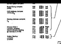
The QED1 example in the listing appears to have some jumper setting differences near both the third and fourth tabs. The CSR block is set left-left-left-right, consistent with the diagram above, but http://www.kpxx.ru/dec/PDP-11/Hardware/DCME-Q4E-F/ClearPoint DCME-Q4E-F-Front.JPG has them set left-left-left-right. What CSR Address would the DEC diagnostics be expecting?

The bottom-most block near the third tab appears to be set as open and then right-right-right-right (the same as in http://www.kpxx.ru/dec/PDP-11/Hardware/DCME-Q4E-F/ClearPoint DCME-Q4E-F-Front.JPG). Those settings suggest to me that perhaps the "window functionality" is disabled in both cases? Can anyone explain what's going on with this aspect of module configuration (Window Size & Location Jumpers)?

At least the pair of jumpers near the fourth tab are explained; seems that the eBay QED1 example module is configured with Battery Backup enabled. I see that http://www.kpxx.ru/dec/PDP-11/Hardware/DCME-Q4E-F/ClearPoint DCME-Q4E-F-Front.JPG appears to be set right-left. Not sure why two jumpers would be employed here; ideas?

I see that 6 modules have now sold; 9 remaining. I wonder where their inventory is coming from?
 
Yeah, the one I got in 2023 had a damaged chip and could not do PMI. If you plug these into a Q/Q slot you will destroy the PMI capability and be left with a normal 4mb board.

On the plus side it uses parity instead of ECC (that's how they fit all the chips on a single board) so it's probably quicker than a DEC ECC board (which does have a performance penalty). In a "hope springs eternal" I just grabbed one for my 11/83.....
 
Yeah, the one I got in 2023 had a damaged chip and could not do PMI. If you plug these into a Q/Q slot you will destroy the PMI capability and be left with a normal 4mb board.
Sure hope that these modules have been treated with proper respect!
On the plus side it uses parity instead of ECC (that's how they fit all the chips on a single board) so it's probably quicker than a DEC ECC board (which does have a performance penalty).
Ahh; I only counted 4 extra DRAM ICs so that would explain it.
 
Yeah, the one I got in 2023 had a damaged chip and could not do PMI. If you plug these into a Q/Q slot you will destroy the PMI capability and be left with a normal 4mb board.
I occurs to me now that the clipped line in the diagram above reads "26 PMI Option Jumpers" which would account for the jumpers adjacent to the first two tabs. It seems that the idea is to remove all of these jumpers and then the QED1 becomes Q/Q-safe. Smart.
 
The bottom-most block near the third tab appears to be set as open and then right-right-right-right (the same as in http://www.kpxx.ru/dec/PDP-11/Hardware/DCME-Q4E-F/ClearPoint DCME-Q4E-F-Front.JPG). Those settings suggest to me that perhaps the "window functionality" is disabled in both cases? Can anyone explain what's going on with this aspect of module configuration (Window Size & Location Jumpers)?
Is this functionality perhaps intended to enable a "bounce buffer" to support 18-bit DMA in a 22-bit system? The default window size of 256KB would be much to large, if so.

Example references to bounce buffers:
https://classiccmp.org/pipermail/cctalk/2018-November/043386.html
https://forum.vcfed.org/index.php?t...rqdx3-to-support-fm-rx01.1209221/post-1209320
 
Is this functionality perhaps intended to enable a "bounce buffer" to support 18-bit DMA in a 22-bit system? The default window size of 256KB would be much to large, if so.
Almost certainly, this is to support 18-bit DMA controllers on systems with 22-bit memory, with support for UMAP registers. This causes the hardware to map an 18-bit address into a 22-bit address space. Almost all versions of RT-11 (except the latest) cannot work with UMAP registers, so some drivers (such as DY) use an intermediate buffer in lower memory.
This is usually required on Unibus systems (there is no such problem on Qbus systems), but there are combined ones - such as PDP-11/84 and PDP-11/94, and such support is needed for such systems.
 
Last edited:
P10-P14 and my DCME-Q4E-F
Code:
P10  X
P11 X
P12 X
P13 X
P14 X

Testing in progress - Please wait
Memory Size is 3840 K Bytes
9 Step memory test
  Step 1 2 3 4 5 6 7 8 9


Message 04      Entering Dialog mode

Commands are Help, Boot, List, Setup, Map and Test.
Type a command then press the RETURN key: MAP


23.996 MHz

Memory Map
Starting   Ending       Size in    CSR          CSR     Bus
Address    address      K Bytes    address      type    type

00000000 - 16777776     3840       17772102     Parity  PMI


Press the RETURN key when ready to continue #

---------------------------------------------------------------------------

P10  X
P11  X
P12 X
P13 X
P14 X

Testing in progress - Please wait
Memory Size is 1792 K Bytes

CAUTION - Memory is Non contiguous

9 Step memory test
  Step 1 2 3 4 5 6 7 8 9


Message 04      Entering Dialog mode

Commands are Help, Boot, List, Setup, Map and Test.
Type a command then press the RETURN key: MAP


23.996 MHz

Memory Map
Starting   Ending       Size in    CSR          CSR     Bus
Address    address      K Bytes    address      type    type

00000000 - 06777776     1792       17772102     Parity  PMI

10000000 - 17757776     2040       17772102     Parity  PMI

Press the RETURN key when ready to continue #


---------------------------------------------------------------------------


P10 X
P11  X
P12 X
P13 X
P14 X

Testing in progress - Please wait
Memory Size is 4088 K Bytes
9 Step memory test
  Step 1 2 3 4 5 6 7 8 9


Message 04      Entering Dialog mode

Commands are Help, Boot, List, Setup, Map and Test.
Type a command then press the RETURN key: #


Testing in progress - Please wait
Memory Size is 0 K Bytes

CAUTION - Memory is Non contiguous


Error 53
No memory in location 0

See troubleshooting documentation


Error PC = 173244       PCR page = 11   Program listing address = 011244

R0 = 020002     R1 = 172346     R2 = 172100     R3 = 000000
R4 = 000000     R5 = 000004     R6 = 172300     Par3 = 070000

Command    Description

   1       Rerun test
   2       Loop on test
   3       Map memory and I/O page

Type a command then press the RETURN key: 3


Memory Map
Starting   Ending       Size in    CSR          CSR     Bus
Address    address      K Bytes    address      type    type


07000000 - 07777776     256        17772102     Parity  PMI

---------------------------------------------------------------------------

Press the RETURN key when ready to continue #


P10  X
P11 X
P12 X
P13 X
P14  X

Testing in progress - Please wait
Memory Size is 3584 K Bytes

CAUTION - Memory is Non contiguous

9 Step memory test
  Step 1 2 3 4 5 6 7 8 9


Message 04      Entering Dialog mode

Commands are Help, Boot, List, Setup, Map and Test.
Type a command then press the RETURN key: MAP


23.996 MHz

Memory Map
Starting   Ending       Size in    CSR          CSR     Bus
Address    address      K Bytes    address      type    type

00000000 - 15777776     3584       17772102     Parity  PMI

17000000 - 17757776     248        17772102     Parity  PMI

Press the RETURN key when ready to continue 

he RETURN key when ready to continue
 
If I understand correctly, then P10 is 1) turning off the window when there is no jumper, 2) turning off memory except for the range of the UMAP window, when the jumper is on the left, and 3) turning off memory in the range of the UMAP window, when the jumper is on the right.
Jumpers P11-P14 - possibly the size of the window, but I'm not entirely sure.
 
If I understand correctly, then P10 is 1) turning off the window when there is no jumper, 2) turning off memory except for the range of the UMAP window, when the jumper is on the left, and 3) turning off memory in the range of the UMAP window, when the jumper is on the right.
How do you think that the left/right settings of P10 would be used in an operational system? I infer that they would be generally useless unless there was an 18-bit addressing DMA device being employed? Is there _any_ use other than in that situation?

Where is the nature of a "UMAP window" documented? I've sampled several OS documents and haven't found a reference to this acronym/concept :-<.
Jumpers P11-P14 - possibly the size of the window, but I'm not entirely sure.
It would be helpful to test other combinations than 1000 for those jumpers. Perhaps 0100 and 0010 to get a sense for what each jumper position appears to determine?
 
How do you think that the left/right settings of P10 would be used in an operational system? I infer that they would be generally useless unless there was an 18-bit addressing DMA device being employed?
In theory, this feature (UMAP) is needed only on Unibus and combined (PDP-11/84 or PDP-11/94) systems, since on QBus systems the memory address bus is 22-bit and there are no problems with addressing on the part of DMA controllers there should be.
Where is the nature of a "UMAP window" documented?
This is a hardware mechanism, support for which is implemented in the OS (say, the RSX-11M used it). Documentation - http://www.bitsavers.org/pdf/dec/pdp11/1170/PDP-11_70_Handbook_1977-78.pdf, page 6-20 (Unibus Map)
It would be helpful to test other combinations
I'll try to think and experiment some more
 
Last edited:
Thank you. Any thoughts as to how the QED1/QED-F might differ from the DCME-Q4E-F? The two main VLSI ICs appear to be the same (CSI 5133 and 5134) although the DCME-Q4E-F appears to use the "A" variants so presumably some improvements there. I've been unable to find any information about either of those VLSI ICs. Possibly there's some "secret sauce" differences in the multiple GALs. Perhaps the differences amount to the switch to the "A" variants plus rebranding for marketing purposes?
 
Back
Top