• Please review our updated Terms and Rules here

DIY Color Computer 3 memory expansion questions/clarifications

Eudimorphodon

Veteran Member
Joined
May 9, 2011
Messages
7,074
Location
Upper Triassic
Another item on my to-do list:

After a working floppy disk controller finally fell into my lap I decided to pull the pair of CoCo3's I've had forever out of storage and play with them. A thing I have rapidly realized is that a 128K CoCo3 is sort of useless for running much CoCo3 specific software. Apparently last year someone was selling a very inexpensive 512K upgrade board called the "Boomerang", but since that source seems to have dried up I'm evaluating if it's worth trying to brew one up myself.

Maybe I'm just bad at Google lately but searching for schematics for a memory expansion came up (mostly) snake-eyes. The CoCo3 service manual doesn't include the pinouts of the connectors, it just shows the original board using 41256s in an inset, but I did eventually manage to find the schematic for a 30-pin SIMM-based homebrew expansion in archive.org's wayback machine that did have the pinouts. Having stared at it all while scratching my head for a while I have some observations, I wonder if anyone here can sanity check them:
  1. It looks like the CoCo3 *sort of* has a 16 bit memory bus? It's confusing on the schematics because they gave both sets of 8 data lines the same designation, but from what I can tell the memory array is wired so all reads are 16 bit wide (there's only one CAS line to both banks of DRAM) and the individual hi/lo bytes are latched in a pair of 74LS374s. The "other" side of those latches goes back to an 8 bit wide bus.
  2. It looks like writes are solely 8 bits wide, coming through a pair of '244 buffers, and there are two separate sets of WE signals for each bank?
From this I now ask the dumb questions:
  1. Does anyone know of a common 256kx8 (or anything in that size ballpark) SRAM that has a multiplexed data bus with DRAM compatible signaling? I just chuck that out there because the "Triad" (and I think the Boomerang as well) say they're SRAM based, but all the SRAMs I know of have non-multiplexed busses, and I don't *see* a latch on those boards to unmultiplex the addresses. Maybe they used a tiny surface mount part.
  2. Looking at 256K x 16 bit wide DRAM parts it seems like the way Tandy did it is a little bass-akwards? There are separate WE lines but a common CAS, so... when a write is happening to one of the 8-bit halves does this mean a read is coming out of the other? (Since the CASes are common.) This seems to rule out just using one of those 256kx16 parts?
Anyway, I have an idea for using either a pair of 256kx8 or a single 256Kx16 SRAM and using a GAL and a latch to paper the weirdness over, but the fact that those other boards *look* like they have just two chips on them makes me feel like I've misinterpreted something. Clarification would be great if anyone's willing to share.
 
I'd be interested to collaborate. I have a tray of 512kB srams to add to the fray and some experience making ram cards. I always thought that the starting point was 16 bit wide srams.
 
I always thought that the starting point was 16 bit wide srams.

Yeah, I'm legitimately puzzled by those other cards saying they use SRAMs because, yeah, at least in five minutes of poking I couldn't find a SRAM (8 or 16 bit wide) with a multiplexed address bus. I mean, the multiplexed bus shouldn't be a deal-killer, my vague idea is just latch the RAS address into a buffer (a 9-bit one, which is a little awkward) attached to half the address lines on the chip while the direct address should be valid for the other half while the CAS signal is active, which is also OE... but if a SRAM that directly accepts multiplexed addresses exists obviously that'd save some plumbing that doesn't seem to exist on those other cards.

And like I said, I also looked at the datasheets for some 16 bit DRAMs, (256kx16s were common on later 512k/1MB VGA cards) but they seem to use a pair of separate CAS lines for hi-lo byte/word selection and a common WE, so it seems like they'd need some glue to deal with the Tandy's different arrangement?
 
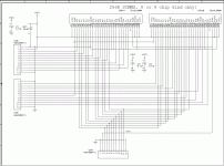
... FWIW, I'm going to attach the schematic for an 30-pin SIMM card I found digging through archive.org. If the creator sees it and wants it deleted I apologize. It is, sadly, the only reference I've found so far for the headers.

Click image for larger version  Name:	512K.gif Views:	0 Size:	33.1 KB ID:	1231717
 
… okay, mystery solved about the “Triad” RAM upgrade, at least. The manual has a close enough photo to read the RAM part numbers, and it’s a pair of plain Jane 512kx8 SRAMs. (Which means it’s wasting half of them.) There is also an installation video on YouTube, and on the flip side of the PCB there’s another square surface mount package, which I’m pretty sure is a CPLD. So it’s probably safe to assume address bus demux is implemented in that.
 
I do need to be careful because if I get a RAM expansion that'll probably immediately gateway-drug into wanting some kind of mass storage adapter...
 
So I finally found the goldmine of Tandy Color Computer RAM expansion schematics.

Here is a SRAM-based RAM expansion for the CoCo3 using a pair of 622048 256kx8 SRAMs from the Canadian CocoNut's user group.

(Editorial note: there are some things about this schematic that I think may be unnecessary? Still mulling that over.)

Also super handy, This Disto manual has the pinouts of the expansion connectors.

(The Disto manual also has the schematics for a board that fits under the 6809 to enable using 1MB of RAM instead of 512K, but I'm not sure how motivated I am to try that, at least right away. It uses four 74LS670s to add a bunch of additional mapping registers and is otherwise pretty heavyweight. I can see why most people who have recreated this sort of thing have gone with CPLDs.)

The question I'm left chewing over is this: the CocoNut schematic shows two complete RAS/CAS address buffers. (Implemented in the form of two 74574s and a 7474 dual flip-flop for the other two bits.) There are other schematics for replacing 41xxx DRAM banks that show only a single buffer, latching the RAS bits and assuming the CAS address will be stable until the completion of the memory cycle. After reading a 41256 datasheet it's clear that the latter isn't necessarily a valid assumption. (The DRAM parts latch the CAS bits on assertion of CAS so once beyond the window necessary to assert that latch they technically don't care if the bits change before CAS is released.) I can't find a datasheet for the GIME that has the waveforms to make this a for-sure decision. However I did find a datasheet for the 6883 SAM (Coco1/2), and according to its datasheet it looks like at least for a Coco2 you would *not* need to latch the CAS address. So if the Coco3 acts like a Coco2 then no latch on CAS should be necessary?

The SAM datasheet also makes it clear that WE is set before CAS. So making some dangerous assumptions here's my idea for using a 16 bit SRAM with byte high/low signals (Referencing datasheet for T55W800FT, but should apply to most others):

1: Schematic will be a single '574 on MA0-7, GAL 16v8 with inputs on MA8, *RAS, *CAS, *WE0, *WE1, outputs on (SRAM) *OE, *R/W, *LB, *UB, A8, and RAS (see below)

2: My recollection is in registered mode GALs clock on the low-high transition. Therefore *RAS will be fed into a combinatorial input pin, inverted, and fed back in as clock on pin1. A registered formula will then latch MA8 on RAS going low, providing 9th bit of RAS address latch.

3: WE0/1 gates *LB and *UB. This is the (effective) truth table for the GAL with regard to control signals:
*RAS*CAS*WE0*WE1=*OE*R/W*LB*UB
LLHH LHLL
LLLH LLLH
LLHL LLHL
LLLL(1)LLLL
(1) I seriously doubt this state ever happens, it wouldn't be useful so far as I know

All other states on the input side result in all "H" on the output side.

Unless there's some timing magic I'm unaware of or we actually need that second latch I think that'll do it in three chips?
 
Does the COCO3 have a "high speed poke"? and if so, do memory cards need to handle this? I think so right?
 
Yeah, the 2Mhz speed is "official" in the CoCo3.

Given the video refresh requirements I think mathematically speaking the memory timing is probably in the "fast" mode permanently(?), at least if the machine is in the 40/80 column modes.
 
Back
Top