• Please review our updated Terms and Rules here

Gold Card work...

Joined
Mar 23, 2024
Messages
16
As the master of vaporware, I've successfully not released dozens of Sinclair QL hardware bits and bobs. :) I think it's time that changed. I've done so much work on so many things, and it's time to just go through the large pile of designs and filter them and condense them down into something useful, manageable and manufacturable. Owning the Sandy designs I have a nice base of reference designs to start from.

A few years ago I reverse engineered the Super Gold Card and retargeted the logic to a later and still available CPLD. I made other changes, like dropping DRAM support and using multiple fast 1Mx16 SRAMs, implementing 4 MB easily, and 8MB with issues. The biggest change was to support faster 68030 devices, up to 40 MHz. This was always a dodgy affair, living on breadboards, crashing often because of the limitations of building it on breadboards, but it was handily more fun than the 25MHz 68020 Super Gold Card. Another design I did disabled DRAM refresh on an existing Gold Card, and added 2MB SRAM to replace the DRAM. This did offer a modest speed boost to the Gold Card for minimal cost.

I made a (since independently developed and better than anything I did) CPLD video chip. There is a separate effort that has borne fruit, but my effort only supported mode 4 or mode 8. The CPLD could be programmed with the equations for a single mode, and you were just stuck with that mode.

I've decided now to bring those two projects together into an FPGA to try to make a complete SGC replacement. Instead of using a SGC-style boot ROM to import and edit existing ROMs I think I'll use a custom Minerva install designed to boot in a way that fully supports future native booting into Minerva or SMSQ/E.

I've spouted a bunch of nonsense over the years and only ever released the most basic things I had confidence in. It's time to man up and do something meaningful.

I'll post progress pics here as time goes by. This is a place marker. I won't be discussing it on the QL Forum or discord. I think this is the right place...

Target is:
68020 or 030 at 25, 33 or 40 MHz
4M of RAM minimum
DD/HD floppy interface
parallel port
dual fast serial
PS/2 keyboard/mouse
 
Today I received 50 MC68EC030RP40 so that's nice. I already have 40x MC68882FN40 to pair with them. I also received a couple of trays of ATF1508 in QFP100 package. I already have on hand reels and reels of 74LVCT16245 level shifters and a bunch of 8Mx8/4Mx16 PSRAM. I also have a bunch of 8Mx8 60nS DRAMs, like thousands.... So the question is, 'to refresh or not refresh?'

s-l1600.jpg
 
Over the last week, besides fighting the pick and place that's the heart of my SMD production line, I've been preparing a test bench for this project. I live in the clutter of 20 overlapping projects, and the ADHD has me. So anyway, I started by clearing a little space and getting the basic equipment I suspect I'll need to use during the early prototyping stages.

I now have a bench with a Rigol DHO924, HP bench PSU, Uni-T bench PSU, and a stonking huge Agilent 16702b logic analyzer with 128 channel logic analyzer and a couple of high speed oscilloscope cards. Rounding out the test equipment is a nanoVNA that will be used to check EMI/RF considerations as the project progresses.

I've also pulled out some components that might be useful for the project: some assorted 68020 and 040 models. Some with MMU, some EC variants. Some 68882s. A few different ATF1508 options in PLCC88 and QFP100 packages. A couple of Tang Nano 9K, on which I'd like to reimplement my video system of a few years ago. A few choices of RAM, from lowly 512Kx8 SRAMs to 8Mx16 PSRAMs to some FPM and EDO DRAMs. The 030 and 040 support burst cycles, so if I can find memory that supports it I would like to implement the necessary logic to speed things along.

Another thing I've needed to do is look at a couple of different QL clones and CPU upgrades to look at the memory maps they used. The QL originally came with a 68008 - a 68000 in every respect except it has an 8-bit data bus. The CPU is internally fully 16/32 bit, just the data bus is hobbled. At the time it was a great way of spooning a 16/32 bit CPU onto an 8 bit data bus in a world where most peripherals had 8-bit registers and ports anyway. The other limitation of the 68008 is it only brought a partial address bus to the outside world. 20 address pins, which means you could access 1MB addressable range. An earlier expansion I made replaced the 68008 with a 68SEC000 strapped to boot in 8-bit mode. This almost entirely recreates a 68008, but with four extra address pins allowing 16MB to be accessed it's certainly a lot more appealing.

This background is important because the operating system, QDOS, was designed with flexibility in mind, but only considered the availability of 1MB address space. An unexpanded QL came with 48K ROM, 16K ROM expansion port, 32K of variable and Io space, 32K of VRAM and 96K of free memory to support the OS stacks, BASIC programs, everything. The first expansion most people got was a 512K RAM expansion, bringing the toal system RAM to 640K. The space above that was reserved for a number of 16K blocks for user expansions - floppy disk interfaces, IDE and SCSI ports, EPROM programmers, you name it. A couple of cards combined a lot of these features on board in a way that left a larger continuous block free, so they could squeeze out an extra few K, with 786K and 896K being the common peak figures in ads.

So now I have to turn all this on its head. The 68030 supports 4 GIGABYTES of addressable space.

More later.
 
I compared the memory maps of the Gold Card, Super Gold Card and the Q-Computers by Peter Graf - Q40, Q60, and Q68.

I learned that the vintage unsupported OS max out at 16MB (Minerva) and even the supported OS SMSQ/E tops out at, I believe, 64MB. This doesn't prevent me from placing devices or etc above that. The OS will just not configure OS resources above that. In the Q40, 60, and Q68, Peter Graf cleverly created a large VRAM and IO area at the top of the 4GB space. This means they're not carved out of QDOSMSQ/E's utilizable area, but they can still work. (QDOSMSQ/E is a way to refer to ALL the QDOS branches and variants in a single, clumsy go).
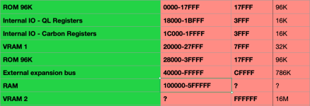
Based on that, and in particular lessons learned from SGC and Q68, my provisional memory map to design hardware around is as follows:

Screenshot 2024-04-12 at 6.14.43 PM.png

192K of ROM space in two areas allows SMSQ/E to run in future, and all the other OS to run out of the box.

VRAM 1 is the original screen 0. VRAM 2 is my 2MB framebuffer and video generator that supports some Q68 and Aurora modes. The internal IO for the system's hardware registers (not QL IO registers) is immediately adjacent to it. I plan to use a SuperIO that implements dual floppy (765-compatible) dual PS/2, dual serial (16450-compatible), real time batery backed clock, and a couple of other little bits. I'm going to need to design carefully to alias everything into sensible places.

The external expansion bus is interesting. The 768K will be divided into 12 logical 64K spaces. The original QL supported 16K expansion spaces. The normal practice was to have a 16K driver EPROM and place a window near the top of the EPROM for the IO space of the device. I have budgeted 64K because it's backwards compatible, and because it allows people to write much more capable and complex drivers, develop expansions that can do so much more, and other reasons I haven't even thought of yet! :p

The idea is that all slots can be occupied, but if only four are implemented they can be slots 0, 2, 4 and 8, giving each card access to 128K, 128K, 256K and 256K. The 4 slots could be jumpered by headers to be 0, 1, 2, 3 giving 64K, 64K, 64K, 576K. Ultimate flexibility. The slots can also be implemented in the 8-bit QL standard interface, or a 16/32-bit capable port using a high density 120-pin connector. The expansion backplane would fit on the mainboard through a high density connector, so a range and choice of expansion backplanes can be offered to meet almost any need. In any case, the cards will meet the Eurocard standard dimensions of 160x100mm.

There is also provision in the expansion area for a card to support four ROM PORT compatible sockets internally.

ROM will be implemented using a large flash - excessively large. It will be 8- or 16-bit, and relatively slow. On boot, the OS would be compied to RAM, then an access to a key address would unmap the flash and write protect the RAM containing OS code. Old school.

The RAM can be implemented in one of several ways. This all depends on how the project develops over time. I see uses for QDOSMSQ/E, but also for Linux, EmuTOS, etc. The low hanging fruit is to use PSRAM. This is spendy but a snooze to implement. It supports burst reads and writes. The next step is to create a refresh engine in a CPLD or FPGA and use EDO RAM. This is cheaper but a little more complex. Finally, if using an FPGA, an IP block for DDR SRAM might be used. This would be by far the cheapest memory but there is a knowledge gap.

More after the weekend
 
You should probably post this on the QL forum, it's a lot more active for QL related things (and Peter, plus a lot of other QL hardware gurus are there and often comment).
 
I made a conscious decision to not post it there but in some parochial place where few QLers might go. I've famously not released quite a few nice bits of kit for the QL. It really is time to pull a rabbit out of the hat, but the kind of input I get there isn't the kind I find terribly useful. It leads to feature creep, unhelpful suggestions, terrific ideas I can't act on, and the withering lack of software help I so desperately need. I think it's far better to build the machine for a more general audience with QLers in mind, and then it can have its own life outside the QL and if QLers want to make use of it, they can.

I have the deepest respect for Peter in particular. His way of thinking is so alien to mine, though.... And I do reach out and ask specific questions within the community when I need to make a decision that can affect compatibility, or just makes things easy for everyone by coinciding with an existing method or layout.

I live in Texas, and as a VCF SW show sponsor and exhibitor I think it's important to eat the dog food, to quote an IBMism.
 
I see. Yes, there are some characters there who can seem curt and sometimes rub people up the wrong way. I don't think they mean it and I have grown to like all of the regulars very much. Apart from the Facebook group though, I think it's one of the only places with any QL related activity. But I'm sure it's fine if you just want to post here... I'm not particularly tech savvy but will watch with interest.
 
As this board is designed to fit in a MicroATX format there are some elements of the design that are defined by standard. One is the IO area. I have put a lot of thought into what is basic and what is optional IO. I quickly decided that there are certain elements any modern retro computer must have: keyboard input, serial IO, and a mass storage interface. There are also some "nice to have" ports and features that I consider basic requirements but others might consider completely optional: mouse, bi-directional parallel port, and a real time clock.

To provide some consistency, and to make sure the machine doesn't become a never-ending hunt for rare or unobtainium parts I have decided to use an ISA SuperIO to provide many or all of these basic features. The Q40 and Q60 did this with a modest SuperIO too, and this made porting SMSQ/E quite easy between models as the IO interface was uniform. I looked for a SuperIO that needs to meet several requirements: provides most or all of the required interfaces, has a flexible front end, is readily available from secondary sources in bulk, and isn't too expensive.

On the subject of porting, I suspect there will already be Linux and BSD drivers for this class of SuperIO that will make producing drivers for various OS 'relatively easy.'

I found a SuperIO that fit the bill and have been building up stocks of several hundred pieces over the past short while. The National Semiconductor PC87307. It supports ISA, EISA and MCA. It has a PC8477-compatible floppy controller, two 16550-compatible UARTs, two PS/2 ports, a real time clock with battery backup, IEEE1284 bi-directional parallel port, power management logic, GPIO and an X-Bus port. The chip is plug and play friendly and PC97-compliant. This means it should be relatively easy later on to pick any other SuperIO that is PnP and PC97-compliant and port existing drivers to work with a new SuperIO very quickly.

I think this is a sensible on-board feature set that just leaves us looking for a video subsystem to round out the basic required feature set. I am less sure that video belongs on the mainboard. Different OS and applications suit different video solutions. Some will simply need a serial terminal. Others might look for a VDP that takes care of letter/graphiucs handling for them. Yet others will demand a very flexible any bit depth any resolution VGA output bitmap display with a large frame buffer. So for now I am going to leave the video subsystem to be the first expansion card. What kind of video would you get the most use out of?

Back to the SuperIO:

The PC87307 (VUL) has flexible and configurable IRQs, base addresses for each utility, and on board DMA controllers.

The floppy controller implements software compatibility with the PC8477 floppy controller. This is a superset of the DP8473, PD765A and the N82077 that we're already very familiar with. The controller supports 8-bit DMA, has a 16-byte FIFO, and supports 5.25" and 3.5" drives.

The PS/2 ports are compatible with 8042AH and PC87911 microcontrollers with 2K of dedicated ROM and 256 bytes of RAM. They support both interrupt and polling.

The RTC has DS1287, MC146818 and PC87911 compatibility. It contains 242 bytes of battery backed CMOS RAM in two banks that we can use for presets, config, preferences, etc.

The chip can provide power management triggered by serial activity, a power switch, or under software control - the OS can turn the machine off.

Two UARTs of the 16550A type, which can be placed in 16450 mode. Standard rates up to 1.5 Mbaud. IrDA. 8-bit DMA support.
A bidirectional parallel port with DMA support. Demand mode DMA. WPP1.9 IEEE1284 compliant. Mode 4 ECP.

16-bit GPIO port. X-Bus data buffer to 8-bit ISA port. Clock source is 32.768 KHz crystal. External 24 or 48 MHz clock input can be used to generate all required internal clocks.

The chip is a 160 pin QFP.

Datasheet: https://theretroweb.com/chip/documentation/pc87306-mar1998-6419bc96b5cee855091194.pdf

I think that gets us off to a good start for a minimal system with functional IO. I do think the one thing missing from this is a basic HD port - IDE is simple to implement and use and has a very low component count. SCSI is simple to implement and use and requires a SCSI controller IC. SCSI does allow for more variety of devices and for 7 logical devices per interface, but IDE is much cheaper and easier to access. What do people think of those two choices and any pros and cons of each?
 
Any system that has ever gone anywhere and that wasn't portable/pocket-sized has some form of expansion. Maybe a cartridge port, maybe an expansion bus. The maximum capabilities of a machine always come through the addition of custom hardware to either add missing desirable features, or recently in the retro computing era, to fix or overcome failings or expiring tech - eg: bypassing UHF video, or providing modern storage. Most 680X0 computers had as a basic a half way decent graphic capability and many used VGA or TTL RGB video out, so that's easy to work with. Almost all had a floppy interface and later an ST506 or IDE interface.

One characteristic of the mid-range 680X0 family is that they support cycles that can transfer 8, 16, or 32 bits on a per cycle basis. Motorola called this feature Dynamic Bus Sizing. This was a surprisingly important feature. It allowed the processor to use cheap and plentiful 8 bit memory and IO devices like UARTs or floppy controllers, or upgrade to 16 bit IDE or do full 32 bit transfers with memory or to custom devices. Additionally, the CPU could do a block of consecutive reads or writes to naturally incrementing addresses much more quickly. Instead of 12+ cycles, they might be completed in 5 or 6 cycles. The burst read/write capability could really help the machine to power through block moves.

The machine I came from, the Sinclair QL, has a 68008 processor and an 8 bit expansion bus. The processor can only address 1MB with its 20 address lines. One of my earliest expansions of my modern design era was to replace the 68008 with a 68SEC000 booted strapped in 8-bit mode. This effectively adds four address lines, allowing the processor to address a 16 MB range. While this is satisfactory from the I Have More Memory Than You™ standpoint, the accesses are still a miserable 8 bits at a time.

For this reason, I think it is important that the new machine have an expansion bus that can fully support and implement Dynamic Bus Sizing. Any card should be able to use any of the bus widths which most suit its purpose. One of the neat elements of DBS is that the CPU commences a write and pouts an address on the bus. The hardware being addressed can assert pins to declare the port size it supports. The CPU then transacts in that port size, and also has two pins to the enabled port indicating which part of the write it is doing. For example, on a 32-bit write, a port might declare its size as 8-bit. The port connects its D0-7 to the bus D24-31. The CPU writes D0-D31, then on the next cycle it scrolls the data up so D16-23 is on the D24-D31 lines to be latched. Then again with D8-D15, and finally with D0-7. The CPU knows the port size, and the port (whatever it may be) knows which byte, word or long word is on the bus. If you have a floppy or UART port, 8-bits is most common. 16-bit flash or an IDE port would get their native word. Long word width fast RAM gets the whole width of the bus every cycle.

Knowing the above, one thing becomes clear. The 64-pin DIN connectors are not going to be enough for 32 data, 32 address and however many control and power/ground lines we're going to need.

I looked at 96 pin DIN connectors as a natural progression, but it's just too tight. I started a Discord to discuss this proposed bus. It started as something more generic. Alas, a bis that tries to be all things to all people, expansions and CPU architectures ends up being a port by committee that doesn't satisfy anyone. I headed off and decided to refocus on just 68K, and on attracting the kind of user who would actually develop hardware and find use for the machine. This is the best way to have a dedicated few come together and make their own dev team. :D

I ended up selecting a more modern high density 120 pin connector that is fully sheathed on the male and female sides - I honestly can't tell which is which though. They strongly support and stabilize the card, support very high speed transfers, have good current carrying capacity, and importantly, 24 more pins than a 96 pin DIN connector for slightly less cost. They also occupy less board space.

Backplane: https://www.mouser.com/ProductDetail/656-TX24120R6STH1E
Expansion: https://www.mouser.com/ProductDetail/656-TX25120PLTH1E

The other element I need to decide on is should the expansions ALL be this type, or should slots be implementable in the format of other machines from the past? Do I put them on the mainboard like PCI or ISA slots, or to I have a "everything connector" so people can add a backplane in the format they desire? For most of the machines I am interested in, the cards are often Eurocard shaped, 160x100mm, with the DIN connector and the expansion ports on the short edges. I think if I put an "everything connector" parallel to the case rear and have a backplane riser, people can place whatever connectors in whatever position they like. I can arrange it so that a card inserted into the backplane will sit inside the rear case wall, 160mm spaced. That places the connector approximately 170-180mm from the back edge of the board. Measuring and iteration might be required there.

If you'd like to join the Discord and take part in the discussions about a 68K flexible expansion port, you can join us here: https://discord.gg/d6jcGTsc
 
One thing that has become increasingly true in recent years is that if we're to build satisfactory machines we need to have multiple power domains. All the cool vintage-relevant systems benefit from using 3.3V components. 3.3V (3V3 from here on) memories are larger, cheaper, and less power hungry than 5V. 3V3 video subsystems open up a lot of options that don't exist in 5V land. This set me on the path of thinking about power design.

As the board will fit any miniATX enclosure, it can also take advantage of the ATX power supply standardization. In line with that, several years ago I bought over 1,000 Molex ATX-24 connectors. ATX PSUs provide all the right volts in all the right amperages. Modern PSUs for several years now have had plentiful 3V3 supply. So it makes sense that I would stay with ATX standards and use an ATX PSU also. Even the grandest of 680X0 systems would probably only need a 300 or 350W supply. A more regular system might only need a 100 or 150W supply. That would massively simplify the design - especially as modern PSUs have a meaningful POWER_GOOD signal that makes it easy to hold the system in reset until the power rails have all stabilized.

I was approached off-thread by someone who asked if I would implement IDE or SATA. I consider IDE spinning rust hard drives to be a poor technology to adopy these days, if only because the drives are getting old and failure rates are starting to go up. So it seems likely I'll implement IDE, and from there implement a JMicron JMH330 or similar IDE to SATA bridge. These support various IDE/ATA modes, and provide transport, link and PHY layers. Being driverless and transparent, each IDE port can be used as IDE or as SATA but not both. For this reason, I will likely implement two IDE ports with master/slave support or four with master only support. Of these, likely only two will support SATA. On reflection, I think the smart move would be to use M.2 SATA cards rather than the 2.5" format. The drives are becoming more common and cheaper compared to their 2.5" counterparts. For most purposes, the 100Mbits/second typical transfer rate will always be enough to saturate any 680X0's bus.

The final short continuation is about the memory subsystem. I have a desire to keep it modular and replaceable/upgradeable. This has led me to a couple of dark corners. One idea is to simply put all the RAM and ROM on expansion cards on the expansion bus. This has a certain traditional "big iron" quality to it. It also comes with some costs - notably that signal handling needs to be much more closely considered. The longer lines might force the introduction of wait states, delaying /DTACK while waiting for transmission oine effects to stabilize. Any good design should moderate this as much as possible anyway. The other idea is to use memory cards but in a non-standard way. EG by using SIMM slots that are readily available, but using custom memory cards that alos contain the memory handling hardware. This way PSRAM, SRAM or DRAM could be used, with the DRAM's multiplexing and refresh handling all dealt with on card. This would also make mixed voltage domains easier. However, this also feels a little clumsy and carries risks if there needs to be too much componentry on a SIMM card. Maybe on-board buffers/level shifters with a 5V/3V3 jumper and a memory expansion connector right up on the CPU and SuperIO might be the way to go? This would provide the best environment to implement trouble-free DMA, keep signals short and clean, and maximize flexibility for the future.

The previous paragraph sets me to starting to consider the possible board layout. The IO area and expansion area are defined by miniATX dimensional requirements. The power supply/filtering area is suggested by enclosure design and PSU cabling to be... Well, we need an orientation system so I always visualize the miniATX board with the expansion ports and IO area at the top/back, and the innermost edge of the PCB at the bottom/front. The CPU, memory and SuperIo need to be in close proximity to each other. The CPU needs to be relatively close to the expansion bus. The expansion bus total length in a fully expanded system should be shorter than 8"/20cm or so.The longer the bus, the lowest maximum speed and the worst transmission line effects can be. This is just one element to the design but it is an important one. This infrastructure has to support any 68K from the humble 68008/8 to the stonking 68060/80.

I would like to release all this hardware under an open license. I would also like to make it and have others make and contribute. There are a number of licenses. I'm looking for one that lets me release all files to buyers so they can understand, maintain and improve their systems. I'd like the license to encourage but not enforce feedback into the project for improvements and new developments. Looking at other projects that have been successful, I have often seen forks and original projects have bad blood between them. I would like that to not happen. I don't know if I mean "I would not like competition" or "I would not like bad blood." I'd prefer co-operation. I'd like people to create an expansion ecosystem around the bus in the same way that RC2014 has an entire ecology based around that bus. So maybe a personal/no commercial license would suit better - though I would definitely want people to co-operatively make and sell for the ecosystem. I just don't know which license best carries that intent and still gives people 100% ownership and transparency of their systems. I suspect a "release clause" that says if I die or request it be so, the entire project becomes completely open without limitations. I think my biggest fear is making something good and then someone else undersells me so I lose money so I can't go on to develop more for it. I don't want to profit, but I don't want to go broke either.

What do you think would be a sensible license to cover that big mess of feels and insecurities?
 
With a little more thinking, one of my earlier ideas above has been ruled out as impractical. The idea of having a processor direct slot so to speak, and have the backplane plug into that. This would require cards to move down into their slots <i>and</i> back into their connectors simultaneously. Each move blocks the other. Instead, I think the board can just have either an open area where people can link up the options of their choice.

Rational options include:

ISA - EISA: These busses are quite slow with master clocks of 8MHz and 10 Mhz. The peak throuput of a 32-bit ISA slot is only a theoretical 32MB/sec. eISA supports bus sizing in a limited way. IT can also be free run at higher speeds but most existing cards will fail at some point.

MCA: IBM, really?

PCI: 33 and 66MHz versions allow 133MBytes/sec, which is more in keeping with a 680X0. Interrupt handling is clever, but also requires some custom logic to translate card interrupts to 68K system interrupts in a useful way. I'm sure people have ideas.

68K processor bus: Runs at CPUCLK so can always transfer whatever the bus can move. Would need a more generic connector than Apple used, which is valued over gold.

NuBus - NeXTbus: A multiplexed bus with unusual enforced hardware mapping of the memory map. This is fine if only using 32-bit systems but we do not want to ignore our 16 and 8 bit brothers and sisters. 68008 and 68010 are processors too!

VME: Tries to be all things to all men. Super extensible. Not really ATX case friendly.

A version specific bus: Maybe Zorro II or III, or QL interface (8-bit and extended?) or an ST bus or etc?

I'm open to ideas/thoughts. For me an ideal bus will support 5V and 3V3 IO - maybe the bus will be 3V3 and all IO needs to be 5V tolerant? Or all cards at 5V and consider 3V3 LVTTL valid? What do you think? Having mixed cases in the system open up a whole range of 3V3 IO, memories, display options, etc. I'm already working on a video card that has 3V3 and 1V8 power domains for this system.

On which note: in an effort to encourage people to produce drivers and bring-up code for these features, I am working on two little engineering sample cards: one brings larger RAM, a faster CPU and the video subsystem to the Sinclair QL. The other brings the 87307 SuperIO to the QL too. With drivers for these, all the QL parts of the system are no longer required for a basic functional system. This would make a native QDOS or SMSQ/E system a small leap for community effort. These designs will also easily be portable to the Amiga/ST. The Amiga has a vibrant but very weird CPU upgrade design philosophy. The Apple SE/30 also has a lively upgrade culture. A friend makes 50MHz 030 upgrades for that which have a transparent tagRAM cache system. Generally, that type of cache works great as long as there's no DMA activity. I plan to have DMA hardware support and whichever guest OS wish to use it can.

Thoughts?
 
I cannot contribute much (don't even have a QL) but I recently found out about the SuperIO and thought about how it could be used with or for an old computer. I hope you can finish the project in some way or another
 
There are many SuperIO. The fun part is that most have a compatible group of parts that use verty standard interfaces. I love that the ISA SuperIOs are usually plug and play compatible for Windows 95, which means they all have a consistent register format. It's also great that the floppy, serial DUARTs, PS/2 ports etc that they provide all use a very standard register set used by other discrete components.

Yes, this helps all 680X0-based projects by opening up new low-component-count and low cost IO options to all of us. In most cases nowadays, SuperIO cost less than a single discrete UART. I'll work hard to make sure the work completes and that the results are Open and human readable!
 
YA, to use a Super I/O chip from an Intel based PC clone would be the ideal way to go.
Easy to interface to other microprocessors and should still be easy to get a hold of (in small quantiles).
..
As far as an expansion bus standard for a updated QL clone, there is some decisions to be made there. But personally I
have hade issues with all the older Sinclair QL clones that others designed. Basically some lack of full compatible with my old
original Sinclair QL hardware and or Custom OEM made software for the Sinclair QL.
..
Ideally it would be a good place to start with enhanced versions of the original systems bus connectors that have full backwards compatibility.
At least with the 16-bit ISA bus and/or the processor direct slot in a Apple Mac SE computer there easy to design replacement boards for them.
It is Easy to add the 32-bit EISA data and Address bus extensions to the standard 16-bit ISA Bus without the extra shared logic support for full
32-bit EISA bus standard.
..
To go with a PCI bus will give the system the latest access to new PCI based peripheral cards, but the logic and programming skill needed to this
will add lots to the systems development cost. Most PCI based cards you can still do the same as them with cheaper newer designed ISA-bus cards
as a alternative. Trying to get a steady supply of PCI bus controller on a regular order bases in a small quality is going to be an issue.
Most of the newer external PC related devices are all USB based now days, So a couple of USB ports would be really use full.
..
I would like to see a Advanced ROM cartridge port, Microdrive port, QLAN ports, and enhanced expansion bus on the unit.
As far as memory expansion is concerned just use a standard PC or PC type laptop based memory expansion slot. This might take some additional
logic to do this, but that would be worth it in the end.
..
Hopefully this message gets other interested in your project as well.
 
Last edited:
I see. Yes, there are some characters there who can seem curt and sometimes rub people up the wrong way. I don't think they mean it and I have grown to like all of the regulars very much. Apart from the Facebook group though, I think it's one of the only places with any QL related activity. But I'm sure it's fine if you just want to post here... I'm not particularly tech savvy but will watch with interest.
Ha if you have an external Quest made QL Firefly Hard drive and or a Quest made OScard then please message me directly.
..
I had a Sinclair QL computer for years now and once used it lots, but it has been pack away for several years now.
Mostly do the cost of upgrading the unit and finding the parts I needed. So it was parked back into storage.
 
I compared the memory maps of the Gold Card, Super Gold Card and the Q-Computers by Peter Graf - Q40, Q60, and Q68.

I learned that the vintage unsupported OS max out at 16MB (Minerva) and even the supported OS SMSQ/E tops out at, I believe, 64MB. This doesn't prevent me from placing devices or etc above that. The OS will just not configure OS resources above that. In the Q40, 60, and Q68, Peter Graf cleverly created a large VRAM and IO area at the top of the 4GB space. This means they're not carved out of QDOSMSQ/E's utilizable area, but they can still work. (QDOSMSQ/E is a way to refer to ALL the QDOS branches and variants in a single, clumsy go).
Based on that, and in particular lessons learned from SGC and Q68, my provisional memory map to design hardware around is as follows:

View attachment 1277738

192K of ROM space in two areas allows SMSQ/E to run in future, and all the other OS to run out of the box.

VRAM 1 is the original screen 0. VRAM 2 is my 2MB framebuffer and video generator that supports some Q68 and Aurora modes. The internal IO for the system's hardware registers (not QL IO registers) is immediately adjacent to it. I plan to use a SuperIO that implements dual floppy (765-compatible) dual PS/2, dual serial (16450-compatible), real time batery backed clock, and a couple of other little bits. I'm going to need to design carefully to alias everything into sensible places.

The external expansion bus is interesting. The 768K will be divided into 12 logical 64K spaces. The original QL supported 16K expansion spaces. The normal practice was to have a 16K driver EPROM and place a window near the top of the EPROM for the IO space of the device. I have budgeted 64K because it's backwards compatible, and because it allows people to write much more capable and complex drivers, develop expansions that can do so much more, and other reasons I haven't even thought of yet! :p

The idea is that all slots can be occupied, but if only four are implemented they can be slots 0, 2, 4 and 8, giving each card access to 128K, 128K, 256K and 256K. The 4 slots could be jumpered by headers to be 0, 1, 2, 3 giving 64K, 64K, 64K, 576K. Ultimate flexibility. The slots can also be implemented in the 8-bit QL standard interface, or a 16/32-bit capable port using a high density 120-pin connector. The expansion backplane would fit on the mainboard through a high density connector, so a range and choice of expansion backplanes can be offered to meet almost any need. In any case, the cards will meet the Eurocard standard dimensions of 160x100mm.

There is also provision in the expansion area for a card to support four ROM PORT compatible sockets internally.

ROM will be implemented using a large flash - excessively large. It will be 8- or 16-bit, and relatively slow. On boot, the OS would be compied to RAM, then an access to a key address would unmap the flash and write protect the RAM containing OS code. Old school.

The RAM can be implemented in one of several ways. This all depends on how the project develops over time. I see uses for QDOSMSQ/E, but also for Linux, EmuTOS, etc. The low hanging fruit is to use PSRAM. This is spendy but a snooze to implement. It supports burst reads and writes. The next step is to create a refresh engine in a CPLD or FPGA and use EDO RAM. This is cheaper but a little more complex. Finally, if using an FPGA, an IP block for DDR SRAM might be used. This would be by far the cheapest memory but there is a knowledge gap.

More after the weekend
I wasn't going to reply to this entry but I decided may I should as others haven't.
..
You should also look at the ROM memory paging system that the AURORA card used.
The old SUN 1 and 2 workstation logic designs is worth looking at if you can find a extended memory board schematic for one. (This board allowed for memory to be above the 16M range on a 68000 based microprocessor).
The older sun Workstations also use the microprocessors FCx status signals. Older (Bate) versions of the Sinclair QL also used them more fully then the on the newer issues 5 to 7 units.
 
Back
Top