• Please review our updated Terms and Rules here

Home-made memory expansion board prevents booting from floppy disks?

if you look on page #6 of the ‘4008 datasheet the graphs imply that with a “CE controlled write” (which is the mode you’re running in if WE is asserted first) WE should stay low *at least until CE goes high*. With your design CE lags WE, so it follows that there’s going to be a few nanoseconds here where CE lingers low *after* WE has already transitioned. Which is technically out of spec for that access mode?
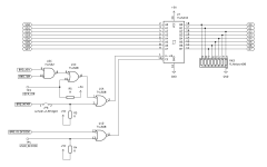
Thats an interesting point, but I have a different interpretation. One thing I have learned is to never consider a timing diagram to be to scale, and to always look at the figures! :LOL:

Case in point, the CE controlled write timing diagram has TCW being represented as shorter than TWP, but in the table of timing figures, TCW is a longer time than TWP...

Back to the point, in the tables on page 4 there are no timing constraints listed between OE/WE/CE specifying how soon before or after these signals can transition with respect to each other for the beginnings and ends of a cycle. For WE and CE controlled writes it only depicts that one should fall before the other, but it doesnt specify how soon. Note #2 on page 6 says that a write occurrs when both CE and WE are low, so I dont think it matters if I start with a CE controlled waveform and end with the depiction of a WE controlled waveform, as long as WE and CE were both low when WE goes high to effect the write.

Data hold time for a write is 0ns after WE goes high, so I suspect that with my decoding I get at least some time after WE goes high where the data bus is still enabled towards the RAM, and thus the write is able to complete successfully in any case. But there doesnt appear to be a problem writing to the RAM anyway, nothing shows any signs of corruption, memory tests pass, and it will happily run all day out of that RAM.

Maybe I need to build another board with just the memory expansion on it to see if perhaps some simpler circuitry is any better. Perhaps there is too much noise emanating from this board as it is?

Its a real head scratcher. :(
 
Last edited:
Maybe I need to build another board with just the memory expansion on it to see if perhaps some simpler circuitry is any better. Perhaps there is too much noise emanating from this board as it is?

Honestly that's what I think is going on. The nits I've been picking about your RAM decoding thing are pretty much just coming from a general hesitation about adding complication where it isn't strictly necessary; the fact that the board seems to work fine when the CPU is driving it indicates that the timing is forgiving enough most of the time, but it still sort of seems to me that you're artificially narrowing a timing window when you don't have to. And just *maaaybe* there's something about DMA timing that's managing to trip it up?

The memory on this board is sharing this buffer/on-card bus with I/O devices, correct? You're absolutely positive that all the chip selects for the I/O devices are qualifying themselves on AEN? The middle of a DMA cycle is where not qualifying on AEN is going to bite you.
 
FWIW, I have a vaguely similar story of mysterious sharing-the-bus issues, although I never actually did figure it out. One of the prototype boards I made for my Tandy 1000 project combined the 16552 UART and XT-CF adapter onto one card (my initial thought before getting super ambitious with the GALs and going to one card to rule them all was to split memory and I/O devices across two piggyback boards, so I could spread the discrete decoding logic across more area), and I thought it'd be fine/good practice to put the UART behind the same '245 that sat in front of the CF port.

Long story short, the resulting card seemed to work fine for everything I threw at it, IE, driving a mouse, Xmodem transfers with Procomm, a PPP client... except for DOS Kermit. For some reasons transfers with Kermit would go into a death spiral of errors and fail. What's odd is they worked perfectly correctly on a previous version of the card that was separate from the CF adapter (IE, part of a three board stack), and the only difference between the two was the buffer in front of it and the 74HCT08 that combined the CE signals for the XT-CF and the UART.

Never did figure that out. I can't imagine how Kermit could be doing anything that changed the mechanics of an I/O read compared to the other programs that did serial I/O, but I didn't see errors anywhere else using the same cables and same hardware handshaking. (I did swap UARTs between cards, problem followed the card.) I wondered if the 10k pull-down that the XT-CF has on one of the data lines could be abnormally loading the UART chip somehow when it was driving the bus, but snipping that out didn't change anything. I didn't have a logic analyzer fast enough to suss out if there might be some kind of significant enough delay in buffer activation to be a problem but, yeah, you'd think realistically if that was the issue you'd see it all the time.

On my final card the 16552 and the XT-CF have had a divorce (the same GAL decodes them, but they no longer share a buffer) and everything's fine again. *shrug*

(I also kept a separate buffer for the memory devices so I wouldn't have to mess with combining direction signals on a single buffer, they're just tied straight to MEMR and IOR respectively, and that also keeps that pull-down I was suspicious of confined to its own little penalty box.)
 
Ahhhhh I think Ive figured it out!

I hooked one of the logic probes up to D0 to look into the timing of data for writes and see what kinds of margins I had during DMA vs CPU writes.

Looking at the capture I could see that during DMA transfers every single memory write to my memory expansion was logic low for D0, and Im like, no that cant be, there has to be something where a byte is written with the LSb set.

And then it hit me like a ton of bricks.

The DMA transfers have IOR/ low to read from the floppy with MEMW/ high to write into RAM. The direction of my data bus buffer is determined by IOR/ AND MEMR/ - that IOR/ for the floppy drive is causing my buffer to output to the system, while the memory gets decoded due to a write to its address which enables said buffer, and then I guess the board outputs something which clashes with the floppy controllers output.

Ye gads. I need to look at my circuitry and try to figure out how to fix this...!

No problem on the nit picking - it forced me to review a lot of details to make sure I understood them and had them correct. And all this talk of memory timing caused me to look a bit further into that and bingo, problem found! :biggrin:
 
Last edited:
Yeah, that is certainly the short stick version.

Im going to need to think a lot harder about how to fix this longer term. And I dont think it'll be an easy fix, not for this board anyway, it is already chock full.

A proper PCB will likely be a lot more dense and I can fit in some more logic to fix cases like this more properly.
 
I took the coward’s way out by sticking with separate data busses for the I/O and RAM halves of the card. No regrets. ;)

FWIW, in the Tandy 1000 HX/EX tech manuals they have the equations for the PAL that (among other things) controls the buffer that sits in front of all the onboard RAM and peripherals. (Conceptually these machines are a minimal 8088 computer with no RAM, and the onboard RAM and peripherals are equal peers on the bus that also is terminated in the expansion slot.) It doesn’t use AEN, it instead uses this garshawful pile of equations that specifically as one of the clauses target the DMA signal used by the floppy controller, but that’s a special case because one of the peripherals behind that buffer *is* the floppy controller, so it *does* need to open the buffer outward during a DMA cycle if it’s targeting RAM not also on the private bus with it.

I think as long as that’s not on the table then just watching AEN should probably be fine; only if your card has anything non-memory on it that might participate in a DMA transfer will you need more than that.
 
Last edited:
I couldn't go to bed without testing if this works and it does! Yay. Floppies now booting with the memory expansion in!

That at least gets me going until I figure out a longer term fix.

And that, children, is why we prototype before going to PCB. 🤣
 
Last edited:
Yes, but in a way that I was not expecting. Lack of understanding of how DMA works on these machines!

Im used to DMA being two operations - one to read from the source and the other to write to the destination, occurring via the DMA controller.

But the Intel chipset works very differently where the source outputs its data onto the data bus, and this is directly routed into the destination. Only memory to memory transfers are done via the DMA controller because only one memory location can be decoded at a time, but peripherals doing DMA can be alternatively addressed via their DMA channel and thus can be "decoded" in parallel with a memory address.

Details! But hey, Im learning.
 
A proper PCB will likely be a lot more dense and I can fit in some more logic to fix cases like this more properly.

FWIW, if you look at IBM's schematics for the IBM CGA card their logic for the buffer direction matches my fix, IE, suppress IOR if AEN is asserted. So that's apparently the "official" solution.

You're not going to need more than that unless you have an I/O device that uses DMA. (IE, actually sits on the DMA 1/3 request lines.) In that edge case then, yes, you would need to assert the buffer in an outgoing direction so data could leave destined for memory not also on your card. (Like that Tandy 1000 case.)

Screen Shot 2023-02-02 at 9.41.27 AM.png
 
FWIW, if you look at IBM's schematics for the IBM CGA card their logic for the buffer direction matches my fix, IE, suppress IOR if AEN is asserted. So that's apparently the "official" solution.

You're not going to need more than that unless you have an I/O device that uses DMA. (IE, actually sits on the DMA 1/3 request lines.) In that edge case then, yes, you would need to assert the buffer in an outgoing direction so data could leave destined for memory not also on your card. (Like that Tandy 1000 case.)
Yeah, nice!

For my proto board I have incorporated one extra AND gate between the AEN OR IOR/ and the AND with MEMR/ that will allow the user to control the direction of the buffer during DMA based IO reads.

My figuring for the new design is:

1. If DMA is reading from memory on my board, MEMR/ will be low which will set the buffer to output, and the buffer will be enabled because my memory is decoded, so that value from my memory will be sent all around the system to which ever destination is reading it.

2. If DMA is reading from an IO device off my board, but writing to memory on my board, IOR is now gated by AEN so the buffer is set to input, and the buffer will be enabled due to my memory being decoded, thus permitting data to be written to my memory. If the write is to memory off my board, the buffer is disabled due to nothing on my board being decoded.

3. If DMA is going to be reading from an IO device on my board, I can configure the buffer to output to the system such that the data can enter memory anywhere that is is required.

I think that covers all bases.
 

Attachments

  • Screenshot 2023-02-03 at 10.52.47.png
    Screenshot 2023-02-03 at 10.52.47.png
    127.1 KB · Views: 5
Last edited:
3. If DMA is going to be reading from an IO device on my board, I can configure the buffer to output to the system such that the data can enter memory anywhere that is is required.

Again, to be clear this last piece is unnecessary unless you plan on sticking something on your board that actually uses the DMA REQ/ACK lines. Are you planning to put a floppy controller, DMA-using disk controller, or soundblaster chip on it? I’m just reiterating this to make sure you’re clear that the PC hardware can’t do DMA to just any arbitrary device.

(You’ve mentioned ”memory to memory” DMA transfers a couple times, which also physically cannot work on the IBM PC/XT; memory to memory cycles with the 8237 have to use channel 0 for the read and, remember, DMA REQ 0 being active causes all the RAM on the board to do a refresh cycle instead of a normal read. You *can* do them on an AT or later; nobody does because they are slower than software block moves.)
 
Yes, I do know. Im just covering all of the bases.

The prototype board should enable you to build anything you want, and I'd like to set it up with the right circuitry to make that possible.
 
Back
Top