- VCF South West - June 14 - 16, Davidson-Gundy Alumni Center at University of Texas at Dallas
- VCF West - Aug 2 - 3, Computer History Museum, Mountain View, CA
- VCF Midwest - Sept 7 - 8 2024, Schaumburg, IL
- VCF SoCal - Mid February 2025, Location TBD, Southern CA
- VCF East - April 2025, Infoage Museum, Wall NJ
-
Please review our updated Terms and Rules here
- Forums
- Companies
- IBM Computers, PCs, Clones and Descendants
- PCs and Clones (XT and early AT class machines)
You are using an out of date browser. It may not display this or other websites correctly.
You should upgrade or use an alternative browser.
You should upgrade or use an alternative browser.
How to Start hardware of 8085up......??
- Thread starter RITESH
- Start date
ArchaicAmusements
Member
I would try connecting SID to ground too, other than that your schematic looks okay to me. I haven't looked at your address decoding however.
Code:
;Flash a LED on SOD
;Top of RAM @ 0x4000

START:  LXI H, 4000h
                SPHL

FLASH:  MVI A, 0C0h
        SIM
        CALL DELAY
        MVI A, 40h
        SIM
        CALL DELAY
        JMP FLASH

;Delay, return to HL when done.
DELAY:  MVI A, 0FFh
                MOV B, A
PT1:    DCR A
PT2:    DCR B
                JNZ PT2
                CPI 00h
                JNZ PT1
                RET
Code:
--------------------------------------------------
8085 DISASSEMBLER LISTING
Line   Addr Opcodes     Label   Instruction
--------------------------------------------------

0001   0000 21 10 40            LXI H,4010H
0002   0003 F9                  SPHL
0003   0004 3E C0       L0002:  MVI A,0C0H
0004   0006 30                  SIM
0005   0007 CD 13 00            CALL L0001
0006   000A 3E 40               MVI A,40H
0007   000C 30                  SIM
0008   000D CD 13 00            CALL L0001
0009   0010 C3 04 00            JMP L0002
0010   0013 3E 1F       L0001:  MVI A,1FH
0011   0015 47                  MOV B,A
0012   0016 3D          L0004:  DCR A
0013   0017 05          L0003:  DCR B
0014   0018 C2 17 00            JNZ L0003
0015   001B FE 00               CPI 00H
0016   001D C2 16 00            JNZ L0004
0017   0020 C9                  RET

---------------------------------------------
LIST OF LABELS
Sorted by address:      Sorted by name:
---------------------------------------------

L0002:  0004            L0001:  0013
L0001:  0013            L0002:  0004
L0004:  0016            L0003:  0017
L0003: 0017 L0004: 0016tingo
Veteran Member
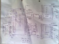
Your schematic is hard to read. Could you put up a better picture somewhere?
Your schematic is hard to read. Could you put up a better picture somewhere?
Hi,
i have got standard schematic by Billo on another forum waiting for finishing exam....
and back to work..!!View attachment 8085SBC.pdfView attachment Ritesh_code.pdf


 I am posting images of 8085 Board.
I have checked all connection are as per schematic and the reset circuit was with pull ups resistance and micro switch connected to GND.
Note:- I found that connecting ROM to board the code on it get changes, why I am using pull ups resistance also at RD and WR pin...
Please help.
http://www.youtube.com/watch?v=qF5gSjhEEM4
tingo
Veteran Member
So, is it working now, or do you still have problems?
per
Veteran Member
The 2864 and 6264 in the PDF schematics lacks most of the connections to the power lines. If you didn't add those, then the two components won't get any power at all, and they'll certanly not work properly.
he 2864 and 6264 in the PDF schematics lacks most of the connections to the power lines. If you didn't add those, then the two components won't get any power at all, and they'll certanly not work properly.
Hello sir,
I think you are right the code in EEROM is getting overwritten don't know why??
My circuit is ad per schematic given above(Pdf).
Hi again,
I was wrong.
the pin behind the group of wire was not clear visible. when i was testing it the WE pin of 2864 i.e. ROM was open, not connected to Vcc that's why my code in EEPROM was overwritten.
I have remove that problem Now i have checked code they were not over written and the SOD pin was blinking LED very fast ..
That mean it is working COOL..!!
soon i will post the video of it..!!
tingo
Veteran Member
Glad to hear that you got it working. ")