• Please review our updated Terms and Rules here

IBM 5100 ROS arrangement

From the disassembled 5100 Executive ROS, here are all the devices it refers to via CTRL $1 (command to access the ROS addresses):

There is mostly #$08 and #$04 as expected, but what are #$02, #$88, #$84, #$82, #$00 ?

Line 542: 03D0 1108 CTRL $1, #$08 (BASIC)
Line 548: 03DA 1104 CTRL $1, #$04 (APL)
Line 2607: 1200 1108 CTRL $1, #$08
Line 4031: 1B6A 1108 CTRL $1, #$08
Line 11066: 502E 1108 CTRL $1, #$08
Line 11999: 55D6 1104 CTRL $1, #$04
Line 12114: 5698 1108 CTRL $1, #$08
Line 12918: 5BEE 1108 CTRL $1, #$08
Line 13361: 5F0A 1108 CTRL $1, #$08
Line 13366: 5F12 1104 CTRL $1, #$04
Line 13371: 5F1A 1102 CTRL $1, #$02 what
Line 13427: 5F76 1188 CTRL $1, #$88 ROS
Line 13432: 5F7E 1184 CTRL $1, #$84 are
Line 13437: 5F86 1182 CTRL $1, #$82 these
Line 13443: 5F90 1100 CTRL $1, #$00 ????

Line 18444: 8000 1104 CTRL $1, #$04
Line 19123: 84D4 1104 CTRL $1, #$04

(recall that whole section around $5FXX is IO Supervisor related stuff; and also only the "CTRL $1,#$02" might be valid, the rest could be bogus/misleading {perhaps actually data instead} -- but doesn't hurt to try 'em all :D )

I think if you plug some of those into the sample machine code for extracting ROS, we'll get some different responses.

And yes, use of those values contradicts the 5100 MIM manual: (where only #$04 and #$08 should be defined)
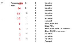
1648536727941.png

I can't find a similar chart for the 5110's use of the CTRL opcode, but in Christian's notes:
"To extract another ROS alter the CTRL instruction at location 0B00, use #$08 for the BASIC ROS and #$02 for the Common ROS." (which is confusing/misleading since elsewhere in the manual, it does say BASIC and Common share the same address space).

Anyhow, that's the request: using Christian's sample to access ROS's, can anyone with a 5100 try plugging in #$02 (i.e. values besides #$04 and #$08) and see if a difference sequence of binary is copied to RWS? If so, that should be the missing ROS. I'm not sure it'll have 6K segments also, but it should be a total of about 18K.
 
Last edited:
I gave them all a go, and no joy.

Note that I have to use a modified version of Christian's program in order to keep the 5100 from loading data "too quickly" from the non-executive ROS. I just stick in some extra NOPs; you can see the code at (where else?) https://github.com/stepleton/5100NonExecutableROSDecode/blob/main/DATA.md

CTRL $1,#$02 -- I looked at all $10000 words. 128 KiB of nothing but $0000.
CTRL $1,#$00 -- I only loaded the first $6000 words, but they were all $FFFF.
CTRL $1,#$82 -- I only loaded the first $2000 words, but they were all $FFFF.
CTRL $1,#$84 -- I only loaded the first $2000 words, but they were all $FFFF.
CTRL $1,#$88 -- I only loaded the first $2000 words, but they were all $FFFF.

I think we've probably got all the ROS data...


(ETA: A previous version of this post said that CTRL $1,#$00 produced a process check, but I think I mistyped it --- I tried it again and got the $FFFF result shown.)
 
Last edited:
Thank you for indulging me. And you don't have COMM, Serial or other expansion card in your 5100, correct? (if it did, then I wonder if a ROS on that card might be available)


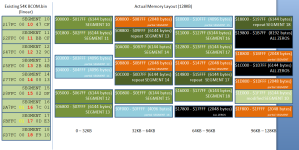
I think I'm a little bit closer to understanding DATA.md notes mean. In your notes, you put together 6K modules -- and these ended up back in the binary file.

But the actual layout/arrangement of the module, as addressed by the system, isn't quite linear (more so for the BASCOM.bin file, where now I suspect: 6 of them are BASIC, 3 of them are for the Common portion -- but not sure which 3 yet -- I'm curious why some of these markers start with "01" vs "00"? similarly for the APL executable,.)


C4 BASIC ROS 32K in diagram, but 36K per Eric Smith notes
BASCOM.binary file arrangement...
$17FC 00 10 47 CF
$2FFC 00 11 BB CF
$47FC 00 12 32 9C
$5FFC 00 13 2B 4B
$77FC 00 14 08 13
$8FFC 00 15 02 DF
$A7FC 01 16 7C 01
$BFFC 01 17 0D E3
$D7FC 00 18 F9 10
( 9 modules + 6K each = 54K filesize )

E2 ROS CONTROL 18K x 8 in diagram (beieve this is 3 modules in the BASCOM.binary)

H2 EXEC ROS 16K x 18 (2 bytes per address? 32K)
H4 EXEC ROS 16K x 18 (2 bytes per address> 32K)
(exeros.binary is 64K filesize)

C2 APL ROS 3 32K
D2 APL ROS 1 32K
D4 APL ROS 2 32K
APLROS.binary file arrangement...
$17FC 00 20 A4 DA
$2FFC 01 21 FC 86
$47F0 00 22 46 D0
$5FFC 00 23 E3 E7
$77FC 00 24 A5 E9
$8FFC 00 25 49 81
$A7FC 00 26 67 90
$BFFC 00 27 13 C2
$D7FC 00 28 FF BF
$EFFC 00 29 E4 45
$107FC 00 2A C1 48
$11FFC 02 2B 7B 65
$137FC 02 2C 58 74
$14FFC 02 2D D9 56
$167FC 02 2E 3D 96
$17FFC 00 2F 99 6E
(16 modules x 6K = 96K filesize)


From Eric Smith notes: http://www.brouhaha.com/~eric/retrocomputing/ibm/5100/

"'control ROS' is part of the PALM processor .... organized as 256 words of 32 bits"

"'executable ROS' is directly addressable by the processor...."
"16Kx18 ...for diagnostic, BUP, IO supervisor and control routines, and virtual machine for BASIC"
"16Kx18 ...provides..virtual machine interpreter for APL"

"'nonexecutable ROS' is accessed as an IO device by the processor..."
"nonexecutable ROS is divided into three regions:
common ROS on the ROS control module 18K
BASIC ROS on one ROS module 36K
APL ROS, on three ROS modules 96K"

Trivia: 8K RWS cards codenamed "Snoopy", the 16K cards used in the 5110 codenamed "Barton".


.
 
Ah, your BCOM.bin isn't "as read from the processor/controller" but is a concatenation of the 9 segments for the "Common and Language" ROS ?

But the notes in your DATA.md are the actual "this-address-gives-me-this-data" result from the CTRL $1 ROS to RWS copy loops?

I think if I just re-arrange your BCOM.bin segments into a 128KB file (per your notes) -- then that should be used as the actual "Common and Language" ROS from the Controller/Processor perspective. I'm still not sure which segments will be the "ROS Controller" (plus it can be "up to" 18K, so perhaps it is just 2 of them instead of 3? maybe that's what the "01" on Segment 16 and Segment 17 indicate?)


I'll give it a shot - just have to splice up the 54KB BCOM.bin file, grabbing the partial segments as described. HxD makes that easy, hopefully can try tomorrow.

EDIT: Understood that this is "non-executive" content - it is executed by the System/3 emulator. But "kick-starting" that emulator I think is part of what the ROS Controller does, which is the portion that the PALM processor does need to run (and access via this binary). And it's very possible that several pins of the address lines can map to different chips or slots (selection pins). I think on the 5110 this was more formally separated (BASIC ROS and BASIC NX ROS, and since the 5110 had more slot-room to work with). Curious to dig into each of those segments and see if they have different "styles" (esp seg 16/17 vs the others)


1648670892114.png
 
Last edited:
Ah, your BCOM.bin isn't "as read from the processor/controller" but is a concatenation of the 9 segments for the "Common and Language" ROS ?

But the notes in your DATA.md are the actual "this-address-gives-me-this-data" result from the CTRL $1 ROS to RWS copy loops?

I think if I just re-arrange your BCOM.bin segments into a 128KB file (per your notes) -- then that should be used as the actual "Common and Language" ROS from the Controller/Processor perspective. I'm still not sure which segments will be the "ROS Controller" (plus it can be "up to" 18K, so perhaps it is just 2 of them instead of 3? maybe that's what the "01" on Segment 16 and Segment 17 indicate?)

You are correct in all of this. In fact, I think I might be able to save you the trouble of assembling the files yourself and provide you with the attached archive, whose ROS files stand a good chance of being accurate to the layout I describe in DATA.md. But I don't recall if that's what those files are, and haven't checked :)

The reason I assembled the ROS data in the way I did is because I think at the time I had some trouble believing (based on some maybe mis-interpreted evidence) that the data were really stored in ROS in the ordering I discovered. Note what I say in DATA.md:

Regardless of the layout of the raw data, it's clear that the segments are meant to be arranged in order in the non-executable ROS (the 5100's "bring up diagnostic" depends on it, for a start). The binary files linked above were made by recreating this arrangement from the raw data.

I don't remember how I came to the conclusion that the non-executable ROS code had a "true" ordering that was different to the one I actually discovered in my ROS recovery, but I think what I did was read the code for the "I" stage in the executable ROS and conclude that it was iterating over each module in order by simply going straight through ROS addresses from one end to the other. To put it differently, I think I thought from the code that the "I" test would fail if the ROS data were truly in the order I discovered in my own extraction process.

I had no good explanation for why the executable ROS would read the data in one way, while my code would read the data in another.

Regardless, I think it's important to keep in mind that there are three possibilities today for us to consider.
  • One possibility is that it's necessary for the ROS data to be ordered in the consecutive way I arranged in my original ROS images. Your experiments with your emulator seems to rule this possibility out.
  • Another possibility is that the data I recovered really does have the "true" ordering, and I was mistaken about the implementation of the "I" test. This will be your next experiment :)
  • A third possibility is that the data I recovered is not the "true" ordering, and neither is the consecutive ordering; instead, there's yet another ordering that's correct that we have to figure out.
From Eric Smith notes: http://www.brouhaha.com/~eric/retrocomputing/ibm/5100/

"'control ROS' is part of the PALM processor .... organized as 256 words of 32 bits"

Just to be clear: this control ROS is not a ROS that we have, but we don't need this data. It's the PALM microcode, part of the hardware that implements the PALM CPU, and since we already have a good PALM emulator written in pure C, we don't need to have any of the PALM's components (including this ROS).

But "kick-starting" that emulator I think is part of what the ROS Controller does, which is the portion that the PALM processor does need to run (and access via this binary).

This sounds right to me. The "common ROS" may contain PALM code and/or data resources that are used by both emulators --- hence "common". Observing the "textures" of the data in the different segments, as you propose, may be quite useful to your deductions.
 

Attachments

  • binary_nonexec_ros_undump.zip
    101.4 KB · Views: 3
Oh, and since you asked:

And you don't have COMM, Serial or other expansion card in your 5100, correct?

Sadly, this is correct. If you would like to write code that tries to bit-bang the ROS data out of the peripheral connection port (that is, the one with the three D-sub connectors at odd angles), then I will run it :)
 
Thanks for those, they look as-expected when compared to the prior ones (the APL one is largely the same except towards the end, and spot checking the "partials" and repeated sections, all look ok in the BASIC one).

Still no go - yet. At least just dropping these "128KB versions" didn't get me past the "18 07". But I'll examine the sections next - if they are different, it could be "mixed addressing" (byte vs word).
 
It may be necessary just to see what address the executable ROS is specifying when it is accessing module 18 in the non-executable ROS. The thing to look for is PUTB instructions that follow the CTRL instructions, like you find at the the start of the program Christian Corti wrote (and I modified) to download non-executable ROS data into memory:

Code:
0B00 1104           CTRL    1, #$04         ; select APL ROS
0B02 D301 000B      LWI     R3, #$000B      ; address of low-byte of R5
0B06 8500           LBI     R5, #0          ; source ROS address ...
0B08 4138           PUTB    1, (R3)         ; ... high-byte
0B0A 8500           LBI     R5, #0
0B0C 4138           PUTB    1, (R3)         ; ... low-byte

(Narrative --- you may know this.) Once you've selected the non-executable ROS that you want with CTRL, you then use PUTB instructions to put in the word address where you'd like your reads from the ROS to start. You need to PUTB two separate bytes: the high byte of the ROS address and then the low byte. In this case we're starting at the beginning: address $0000.

PUTB 1, (R3) means "put the byte stored at the memory location kept in R3 into I/O device #1". There is no other addressing mode available to PUTB --- you have to use this register-indirect addressing scheme. See the bottom of this page for the code idiom Christian and I are using here.

Anyway, the thing to do would be to look for CTRL 1, #08 instructions (1108), then look for PUTB 1, (R?) instructions just afterwards. Work out the address stored in R? when the "I" self-check is trying to access ROS module 18, and that's where the module 18 data belongs.
 
Not giving up, but taking a break to address some other projects (including some 5110 stuff!). Hopefully can study the CTRL and PUTB as you've described next week. I do agree we're close, as everything needed should be present.
 
Last edited:
Pulling on this thread again...

The 5110 ROS's were extracted as 6x ROS files - one for the Executive ROS, then 5 additional ROS binary files.

The 5100 ROS's were extracted as 3x ROS files - one for the Executive ROS, then 2 additional ROS binary files.


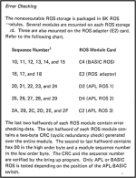
The 5100 MIM has more detailed information about the ROS "segments" - for example, the mention of 6KB segments is entirely gone from the 5110 MIM. Or, for example, the 5100 MIM describes what the segments are. In otherwords, the 5110 MIM doesn't have an equivalent to the following details that appear in the 5100 MIM:

1654505879515.png

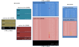
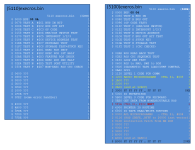
The chart below summarizes the CRC values at the end of each of those 6KB segments (boxes on the right, for both 5100 and 5110). And this is good evidence that the 5100 ROS binaries *are* in the correct order (for two reasons: it is consistent with the 5110 ROS binaries that are working in the emulator, and also that I found this "ALU" Processor Data Flow chart and it is identical in both the 5100 and 5110 -- in otherwords, we know the PALM opcodes are the same between the two systems, and also I believe the same overall data flow and addressing of the system and ROS's is the same {at least per this data flow chart}).


In the 5100 MIM, is calls out "segment 18" as the Common ROS. I don't know if it meant that segment 16 and 17 also are as well - except note in the far right binary_BCOM.bin, segment 16 and segment 17 are prefixed with "01" instead of "00". This appears in a few places (across both 5110 and 5100), and the MIM description above says this halfword "contains hex 00 in the high order byte". So that's a mystery -- what do these non-00 values indicate?


Something else interesting shows up in the basicros.bin and aplros.bin for the 5110. Comparing them side-by-side, I noticed right at the 8KB offset of each file, they have an identical hex sequence. Everything else about these two files is quite different. And what are these files, where did they come from? Well, the 5110 system more explicitly calls out a BASIC ROS and APL ROS component. In the 5100, I think these were more integrated as part of the Executive ROS. I can't think of anything special about these 8KB offsets, and I don't think these are CRC values (since the content is otherwise vastly different between those binaries). But the BASIC ROS and APL ROS are what do the emulation/translation (read the mainframe opcodes into RWS i.e. from "non-executive ROS code", and translate it into native PALM, as my general understanding).

I'm still curious why on the 5100 that CTRL 1,#$02 isn't reading any different kind of ROS content. But the 5100 MIM does say the Common ROS is "segment 18" which is part of the NonExecutive BASIC ROS (which should mean PALM and non-native code is all mingled together -- unless segment 18 is strictly just lookup table data).

In any case, for the 5110, the comros.bin is clearly the "segment 40" that you see in the BUP CRC checks.

Another item of interst here is: how is the 16-bit CRC of these segments determined? CRC isn't just something that is a singular standard rule - you have to know exactly what content is being CRC'd, and a few paramters of the function being used to do the CRC. There are dozens of 16-bit CRC "standards." So far none of them line up for me, but again I'm not entirely sure what content is being CRC'd (all the non-00 hex values? the entire 6KB segments? could/should trailing 00's after the machine code count towards the CRC?). Christian Corti has instrumented the 5110 execros.asm with about where the CRC checks are happening, but it's still a bit unclear to me (and eventully plan to circle back and step through that code -- in some register, the number corresponding to the CRC of each of these segments should appear; maybe that's the thing to do, set a kind of "watch" on these values in the registers and trigger off that).


Anyhow, still a mystery on why the 5100 emulator isn't transitioning properly to the Language ROS. But this chart outlines differences between the system. The emulator is coded to look for "commonros" and "basicros" and "aplros" bins.


1654505654459.png
 
Nice to return to this mystery :)

how is the 16-bit CRC of these segments determined? CRC isn't just something that is a singular standard rule - you have to know exactly what content is being CRC'd, and a few paramters of the function being used to do the CRC. There are dozens of 16-bit CRC "standards." So far none of them line up for me, but again I'm not entirely sure what content is being CRC'd (all the non-00 hex values? the entire 6KB segments?

CRC is being computed for the entire 6 KiB segments.

I don't know the details of the CRC algorithm in use, but I was able to write a Python implementation of it. How did I do that? Well, I just wrote some Python code that did the exact same thing as the PALM opcodes in the 5100's executable ROS. You can see the details here in my 5100 non-recoverable ROS write-up:


It would certainly be more elegant to understand the CRC polynomial and other key details, but it's not strictly necessary. You can just keep translating the PALM code into whatever language you please.

I think we may have discussed it before, but officially, the 16-bit CRC of each 6 KiB block is: $0000. That's because each block contains up to (6*1024 - 2) bytes of "real" data, and then the two final bytes are whatever value has to be ingested next by the CRC algorithm to cause the CRC to be all zeros.

(Depending on how you look at it, that final word itself is "the CRC". But what the executable ROS does for a block is: [1] initialise the CRC value to $FFFF, [2] loop over each successive 2-byte word of the block, updating the CRC using the code linked above, and [3] check that the final CRC is $0000. You can find complete Python source code for this here.)

Something else interesting shows up in the basicros.bin and aplros.bin for the 5110. Comparing them side-by-side, I noticed right at the 8KB offset of each file, they have an identical hex sequence.

Interesting observation. I don't have time to find out now for myself, but I wonder if these four-byte sequences are made of pairs of valid PALM instructions?


As for your remaining questions: your guess is as good as mine!
 
Awesome, thanks! I ran that Python on the 5110 BIN's as an exercise, and got the expected results. Sorry I missed this in your notes earlier!


Aside: I didn't realize PNGs contain CRC'd blocks... Came across that while refreshing up on CRC's. I was trying to use CRC RevEng to see if it could reverse out what IBM did here, no luck yet.


There is one minor(!) comment issue in your Python
# RET R8 <-- in all other cases Rx == r[x], so this probably meant RET R9 ??
return r[9]
And indeed it walks across the entire 0x1800 (6KB) stream. Very cool, the data itself contains its own CRC checksum?


Random Trivia: On the 5110, between the cursor blinking ON and then OFF (and vice versa), the PALM executes approximately 90,000 instructions (while waiting for the duration to invert the state of the blinking cursor; this is verified in the emulator). So if it transitions 4 times per second (OFF ON OFF ON), that's around 0.36 MIPS?


Regarding the "identical code @ 8KB" in the BASIC/APL ROS... (they also have a few bytes of identical code at the very beginning)

It's a bit more than just 4-bytes at the end...

Code:
@ first 8K offset... (one byte difference)
1FE0 BASIC: 00 00 00 00 00 00 00 00 81 02 01 1D 81 31 31 E8 31 FC 81 00 01 1D 81 0A 31 FD 08 24 20 50 F0 17
1FE0   APL: 00 00 00 00 00 00 00 00 81 02 01 1D 81 51 31 E8 31 FC 81 00 01 1D 81 0A 31 FD 08 24 20 50 F0 17

@ second 8K offset... (one byte difference)
3FE0 BASIC: 00 00 00 00 00 00 00 00 00 00 00 00 00 00 00 00 00 00 81 02 01 1D 81 32 31 E9 08 24 20 50 F0 0D
3FE0   APL: 00 00 00 00 00 00 00 00 00 00 00 00 00 00 00 00 00 00 81 02 01 1D 81 52 31 E9 08 24 20 50 F0 0D

These should be native PALM instructions, here they are disassembled. My guess is some kind of error handling code, that writes a value to memory to indicate which ROS has had the error?


Code:
1FE8    8102        LBI R1, #$02
1FEA    011D        MLH R1, R1
1FEC    8131        LBI R1, #$31     <-- #$51 for APL ROS
1FEE    31E8        MOVE $1D0, R1
1FF0    31FC        MOVE $1F8, R1
1FF2    8100        LBI R1, #$00
1FF4    011D        MLH R1, R1
1FF6    810A        LBI R1, #$0A
1FF8    31FD        MOVE $1FA, R1
1FFA    0824        MOVE R8, R2
1FFC    2050        JMP ($00A0)
1FFE    F017        BRA $1FE8         <-- maybe this address is an error handler?


3FF2    8102        LBI R1, #$02
3FF4    011D        MLH R1, R1
3FF6    8132        LBI R1, #$32       <-- #$52 for APL ROS
3FF8    31E9        MOVE $1D2, R1
3FFA    0824        MOVE R8, R2
3FFC    2050        JMP ($00A0)
3FFE    F00D        BRA $3FF2          <-- maybe this address is an error handler?
 
Last edited:
BTW, when the 5100 starts, are there any ROS hex codes besides 1X and 2X? I found one video with a 5100+BASIC model, and I think the 5100 starts at segment/module "18" -- then it cycles to 10,11,12,13,14,15,16,17 (I assume in the APL mode, it would cycle to the 2X series? or if BASIC+APL is equipped, it cycles through all of them regardless of the Language setting?).

On the 5110, it starts on the "4X" modules (Common ROS) during the startup checks.

I'd be very curious on an APL-only 5100 if it starts also with segment/module 18.
 
Last edited:
I like your hypothesis of the "identical code" being some kind of error handler. It makes some sense: no matter how big your ROS code gets, you always know that you can jump to the address "at the end" to do... something that needs doing.

I'd be very curious on an APL-only 5100 if it starts also with segment/module 18.

It does. Plus, only the selected non-executable ROS is tested.

This recording of mine shows you what you will see for APL and for BASIC:

The first half is the APL start-up sequence, the second half is BASIC.
 
Hello Everyone,
I can't add much to help here but I'm fascinated by your work on reverse engineering the 5100/5110. I had one on my desk for about a month in ?? Maybe 1975-76. I was evaluating it for use as a tester controller for new chips under development at the IBM site in Vermont. I loved the idea of writing the controls in APL, as I had used APL a lot in analyzing and graphing test results from chips that were in development. I knew the guys in Fishkill who worked on the PALM (Which was used on some internal automated tools). BUT in the end it was Just Too Slow. I needed to test many hundreds of chips per shift.

We had been using IBM System/7's but they were cumbersome and I/O was a monster part of that. I was talking to the guys developing the follow-on IBM Series/1 and it looked really good and modular. I talked to a guy named Don Raimondi who had developed EDX (Event Driven Executive) and the fast interpreted language EDL. I got him to ship me a System/7 disk (2-ft in diameter) that I could plug into a System/7 and run EDX/EDL if I snuck in in the evening :) That was cool, and I even got to send real data up to the System360 hosts. And I was an Unblessed Engineer not IS.

I got the first Series/1 in Vermont and Don sent me EDX on 8" floppies that I installed on the S/1 hard disk. S/1 had decent display and keyboard and I could save code I wrote on 8" floppies. But I needed fast I/O, and the estimate from the developers to produce a fast CycleSteal (AKA DMA) adapter was $28000 and 6 months. The S/1 had a nice backplane, slots for I/O and Memory. There were 4 memory slots and I got two 32Meg cards. IBM made a BREADBOARD card that fit a S/1. What?? All the cards had the same edge connector and power pins. So what if I HAD looked at the (Warning: FOREIGN Processor Reference!) Motorola 68000 manual and found it had NO I/O INSTRUCTIONS. I/O was just mapped to the memory space! Sacrilegious!

So soon I had a couple of 16bit registers and a couple of DACS hanging off the S/1 plugged into a MEMORY slot. And it worked. And it ran 400 Thousand Bytes Per Second. Not I/O instructions, just MOV. in the 6 months I had guys building a backplane and plug-in Digital, DAC, ADC , Counter cards, all on MEMORY MAPPED bus. A friend in another department moonlighted a S/1 card that has optical isolation on all memory and data lines and drove IBM ribbon cable used on S/360. I did have a little confrontation with the IBM "CE" manager. He said I couldn't touch the insides of HIS machine he had to maintain. We had a little meeting with upper management where I waved the bill my department paid of $22,800 for the Series/1. It's IBM's machine, and it's MINE!

Sorry, people, didn't plan that whole harangue.. Um, I DID suggest that some other department make an adapter that plugged into a 8K? memory slot on their 5100. But their manager said NoWay. But 6 months later THEY had a series/1 and asked for our "Shared Memory Adapter" design files...

Vermont Legend has it that the Boy Wonder (Our site executive back then) hacked the 5100 and eventually got to run as a VM operator. Actually he WAS a wonder. And he had friends in Poughkeepsie. My friend Jay L and I were hacking Ohio Scientific machines at home and the site exec would call us on the phone at 11PM to try some data transmission test. But the IBM Hackers is another long story for some PC thread.

Old Guys are Dangerous with all their stories...

Regards, Terry terry@terryking.us terry at BTVMANVM
 
Thanks for sharing, I like hearing how these systems were actually used. IO through the memory slots? That's radical!

The complete 5110 I have was used by a stone company in Chicago. The building still exist, however I think the company may have closed around the 2020 pandemic time (if anyone's in the Chicago area and can check an address, PM me -- it's over a 1000 miles away for me).

I once spoke with Jeffrey Grube of Punxsutawney Electric Repair Company - I think he had 2 or 3 of these systems, but admitted they got replaced by the 5150 in the early 80's. But he did program the 5100's himself as well. I still don't have an estimate on how many of these were actually made (and I've met quite a few folks who said they used one in high school, but I wonder if in some cases they might confuse it with the 5155). I can tell if the 5100/5100's were in the 100's or 1000's sold, I just don't think it would have been much higher order then that. I've thought about making some kind of "IBM 5100 Serial Number Registry" site - if people could be honest about it.


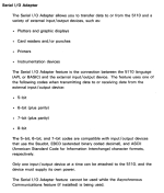
I was reading back through the "General Information Manual" of the 5110, and I came across this in the list of optional features on page 33:

1654680903051.png

A serial IO graphics display, for-real ? And I've never heard of Baudot.
 
Anyway, the thing to do would be to look for CTRL 1, #08 instructions (1108), then look for PUTB 1, (R?) instructions just afterwards. Work out the address stored in R? when the "I" self-check is trying to access ROS module 18, and that's where the module 18 data belongs.

I had tried this awhile ago, but got sidetracked on other projects. So giving it another go, I think I found maybe what you were suggesting here.

In the Executable ROS, I set a breakpoint in work-in-progress 5100 emulator, and found this to be the best match of a CTRL / PUTB sequence that is executed just prior to the "18" module check at startup...

Here is the addresses involved and the disassembled code, and my notes along the way...

Code:
5F0A    1108        CTRL $1, #$08        Since BASIC and Common ROS is same on 5100,  (on 5110, I think CommonROS is CTRL $1, #$02)
                                               R15 = 0108

5F0C    8108        LBI R1, #$08         R1 changes from 5EFF to 5E08
5F0E    CF1A        SNE R15, R1          R15==0108, R1 becomes 5F12  [this is really JHL Jump high or low (not equal)]
                                                     i.e. since R1 and R15 are equal (LO-order bits), R1 = PC+2 (5F10+2 = 5F12)
                                             Larger view: this looks for CTRL $1, #$08 (BASIC/COMMON) first, then APL, then #$02 (which for 5100, #$02 is undefined?)
                                             Since BASIC/Common is found, PC stays 5F10 and we branch to 5F22

5F10    A00F        BRA $5F22        ; $10(R0)

....

5F22    A407        ADD R4, #$08         R4 changes from 100 to 108
5F24    4140        PUTB $1, (R4)+       PUTB at RWS[R4], which is C000    [R4 is incremented from 108 to 109)
5F26    4140        PUTB $1, (R4)+       PUTB at RWS[R4], which is C000    [R4 is incremented from 109 to 10A)
5F28    8E1B        LBI R14, #$1B
5F2A    0EED        MLH R14, R14         R14 becomes 1B1B
5F2C    8E1D        LBI R14, #$1D        R14 becomes 1B1D
5F2E    0F5C        MHL R15, R5          R15 becomes 0101   (R5 is 0100)
5F30    8102        LBI R1, #$02         R1 changes from  5F12 to 5F02
5F32    CF1A        SNE R15, R1          like earlier, does (R1 == R15)?  Since R1 != R15 (LO-order bits), PC becomes 5F36
5F34    A03B        BRA $5F72        ; $3C(R0)

5F36    8101        LBI R1, #$01
5F38    CF12        SE R15, R1
5F3A    A02D        BRA $5F6A        ; $2E(R0)

I believe this $5FXX section is right in the area of the CRC checks you described finding long ago. And as we know, the two "back to back PUTB's" is a full halfword address. As confirmed, the PUTB address involved in the RWS[R4] is $C000 (the expected start of module 18's 6KB).

But I'm still not fully understanding the code - to do a CRC check, don't get GETB to read the module code and do the check? PUTB is communicating the contents of RWS[R4] over to the specified device address ($08)?

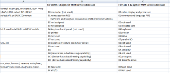
And after a little digging, I came up with this Device Address chart between the 5100 and 5110:

1654684223106.png


What's interesting is how devices 0A/0B/0C/0D aren't described very much -- yet they aren't just listed as not-used. Must be the time machine interfaces :p Teasing, I'm sure they were "work in progress" prototype/experimental device addresses for the features that eventually got added in the 5110.
 
A serial IO graphics display, for-real?

Yes! In the 5110's time, one candidate would have been something like the Tektronix 4010 series, which have a lot in common with plotters.

But I'm still not fully understanding the code - to do a CRC check, don't get GETB to read the module code and do the check? PUTB is communicating the contents of RWS[R4] over to the specified device address ($08)?

I'm not 100% certain of the question, but you do need to GETB the bytes in order to feed them into the CRC. It must be happening elsewhere. It looks to me like this is setup code of some kind in preparation for the check?
 
I think I see the GETB later. But the ROS are read only, so a PUTB isn’t modifying any content of the ROS - so I wondered what it was putting. I suppose in this case it is putting the requested address (c000) in some buffer of the card that holds the common ROS ( I.e. to setup for something I’m about to do with that device )
 
On the quest towards a working IBM 5100 emulator: still not much progress.

I modified the Emulator to handle address breakpoints, and color coded Registers to make them easier to read R0 to R15. Little things (local only, not in the repo).

To recap: the Executive portion is working fine, it's the CRC check that is failing - not because I think anything is wrong with the extracted ROS binary, but because I think the Device Addressing isn't being processed right. I only get a little time in the evenings to plug along.

One thing I decided to do was to compare the Executive ROS between the two systems (5100/5110). At the FTP site mentioned at Christian Corti, I found a disassembled copy of the IBM 5100 Executive ROS that was annotated with comments. Or maybe this was from @stepleton ? Eitherway, I hadn't noticed it before - I had disassembled the 5100 ROS myself before awhile back, but the .asm file I found here had way more annotated notes.

The IBM 5100 MIM calls out some specific addresses in the Executive ROS. Those notes are gone in the IBM 5110 MIM documentation. But with the 5110 emulator and 5100 emulators (such as it is), I've stepped through and verified the annotated notes...


Recall that the extracted IBM 5100 execros binary is a full 64KB. However, it has a large section of 0xFF values at the center (8KB) and end (20KB) - altogether those total 28KB, meaning the IBM 5100 Executive ROS only has 36KB of actual content.


But one thing that got my attention is that whomever had previously disassembled through the 5100 executive ROS, they too asked "why' the code was doing CTRL $1, #$02 ? Or more specifically, they had...

Code:
5F12    1104        CTRL $1, #$04        ; select BASIC or Common ROS
5F14    8104        LBI R1, #$04        ; ??? APL ROS
5F16    CF1A        SNE R15, R1
5F18    A007        BRA $5F22        ; $08(R0)

5F1A    1102        CTRL $1, #$02        ; WTF ????
5F1C    8102        LBI R1, #$02        ; ??? Common ROS
5F1E    CF12        SE R15, R1
5F20    A047        BRA $5F6A        ; error 14
...


Which is essentially what I asked too - why is device #$02 consulted there?


1655546174302.png
 
Back
Top