Upcoming Events:
- VCF South West - June 14 - 16, Davidson-Gundy Alumni Center at University of Texas at Dallas
- VCF West - Aug 2 - 3, Computer History Museum, Mountain View, CA
- VCF Midwest - Sept 7 - 8 2024, Schaumburg, IL
- VCF SoCal - Mid February 2025, Location TBD, Southern CA
- VCF East - April 2025, Infoage Museum, Wall NJ
-
Please review our updated Terms and Rules here
- Forums
- Companies
- IBM Computers, PCs, Clones and Descendants
- PCs and Clones (XT and early AT class machines)
You are using an out of date browser. It may not display this or other websites correctly.
You should upgrade or use an alternative browser.
You should upgrade or use an alternative browser.
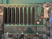
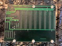
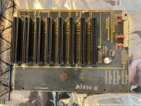
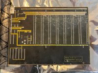
images of the 5161 planar board / backplane?
- Thread starter TRS-Eric
- Start date
TRS-Eric
Member
- Joined
- Sep 28, 2021
- Messages
- 10
Sounds good. Keep me in mind if you ever consider it!
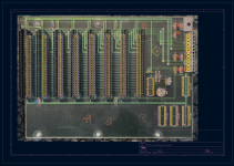
Here's what I've come up with so far from your images. I was able to figure out how to overlay images in KiCad. Would you be willing to give me a precise width and height of the board? And if you have a calipers, what's the thickness? Just for curiosity. With the width/height I can scale the images properly and go from there. I already have the precise measurements of the actual ISA slots so I'll be able to line those up properly.
PS. I know the ISA slot holes are not the right spacing I will get that fixed! Oh, and I plan to open source this design. Is it ok if I include your images with credit?
Rough WIP X-ray image:

Last edited:
TRS-Eric
Member
- Joined
- Sep 28, 2021
- Messages
- 10
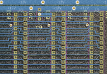
Hi all. I'm pretty much done with the above. I no longer need measurements as I have confirmed with my regular motherboard that everything is accurate. The entire board is accurate to within a few millimeters based on the photos. Here's some finished glamor shots!
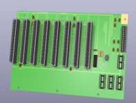
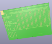
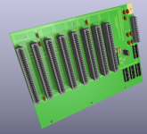
I've left the holes pretty large on the variable capacitor so that one could use any number of different types without too much headache.
I'll release this all on gitlab as soon as I've tested it.
Before I send off however, I just wanted to confirm with anybody who can answer, is the DB0 line not connected to anything? Pin 40. Pin 9 is connected on the other side, but pin 40 doesn't seem to be connected from either side.

jxm
Member
DB0 (data bus bit zero) is required.
It also looks like IO is broken as it passes C9 and C11.
Also the square GNDREF pad of C9 shows as rats nest (unconnected).
Something does not look correct with power connectors P1 and P2. On the PC motherboard the grounds of P1 and P2 are next to each other. In the xray view in post 7 the grounds are on opposite ends. I think they need to be rotated 180 degrees. That is unless something has changed between post 7 and post 8.
Last edited:
TRS-Eric
Member
- Joined
- Sep 28, 2021
- Messages
- 10
C9 and C11 look good here, must have fixed it on the errors check pass. They're connected on the top side and then the bottom side over to pin 1.It also looks like IO is broken as it passes C9 and C11.
Also the square GNDREF pad of C9 shows as rats nest (unconnected).
Something does not look correct with power connectors P1 and P2.
P1 and P2 were probably not in the right orientation at the time of the first pic as that was just a rough layout to get started, they are correct now in the final version.
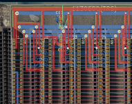
Thanks for checking, I thought maybe db0 was unused but clearly that's not true. I think I see where db0 is run but it'll take over the gnd line, so now I need to figure out how gnd pin 10 is connected. I'm going to study the pictures more.That's interesting, I wonder where the line is hiding. I'll take another look through all the various images.
Jafir could you give me more photos around the third isa slot from the left, there's some traces here I'm not really figuring out. Also if you can test out the ground pins 10 and make sure they are connected, and if you can see how that would be really helpful :D
Last edited:
TRS-Eric
Member
- Joined
- Sep 28, 2021
- Messages
- 10
Never-mind all that. I've reasoned about it ceaselessly and figured out all the traces with extreme confidence!
I'll be ordering and building it soon and will report back (verified tolerances are jlcpcb tolerances). I'll also put it on gitlab once I've verified it works!
Here are the files in case anybody wants to build it with me!
 www.dropbox.com
I'll be ordering and building it soon and will report back (verified tolerances are jlcpcb tolerances). I'll also put it on gitlab once I've verified it works!
Here are the files in case anybody wants to build it with me!
Dropbox - File Deleted - Simplify your life
Last edited:
TRS-Eric
Member
- Joined
- Sep 28, 2021
- Messages
- 10
I'm sorry to keep bumping this, it is too late for me to edit.. I have instead decided to publish it here: https://gitlab.com/trs-eric/5161-planar-backplane-board

