• Please review our updated Terms and Rules here

Mini-Omnibus backplane for debug and minimal system

It seems like it’s converging. Made some updates based on comments, v2 review revision r04.

Changes since v2 r03:
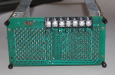
1. All power terminals are now on the top edge, or back of the backplane when mounted in a chassis.
2. Converted all power terminals to Keystone 1257 2-tab terminals. These are more like the terminals on the 8/M backplane. Keystone 1257 is available from Mouser and Digikey. This update supports 4 wire connections for +5V and 6 wire connections for GND, so systems can double or triple-up wires for +5V power. Single quick-connect terminals carrying high current are notorious for burning. My 8/M box has been modified to use 3 wires each for +5 and GND. Also, small debug systems using separate +5, +15 and -15 supplies can connect them directly to the backplane terminals.
3. Converted all mounting holes to use M3 cap screws. This way, fewer part types are required and less copper area is wasted around the mounting holes.
4. Related to Doug’s comment about fitting into an 8/E/F/M chassis, I realized the front of the backplane near the first slot also extended a bit too far forward if mounted in an 8/M chassis, so the front overhang was reduced by 4.5mm.
5. Added a single 0-ohm jumper to enable/disable the on-board Power OK circuit.

Images of the updated top and bottom layers of v2 review revision r04 are here:
Mini Omnibus Backplane layout Top v2 r04 x2.jpg Mini Omnibus Backplane layout Bottom v2 r04 x2.jpg

A summary of the voltage drop on the +5V pins at each connector is in the following plot. Various combinations of the AWG 14 jumpers are shown. Installing only two jumpers is recommended: J7 to J8, and J11 to J12. Installing J9 to J10 provides almost no benefit so I might remove it from the layout. Moving the power terminals to the rear of the board and better layout has reduced the voltage drop compared to the previous version.
backplane v2 r04 voltage drop per connector.png
 
It seems like it’s converging. Made some updates based on comments, v2 review revision r04.
Somehow I managed to miss two iterations of your design! It's better than ever. Thank you for all of the attention to physical mounting, board rigidity, and flexure-cycling.

My only concern at the moment is WRT your earlier comment that "I envisioned that the B and C connector rows would be a single edge connector with pins removed and shims installed."

Could you please identify a practical supplier for these new-length B-C connectors?
(And a reminder for the A and D connectors as well ...)

Thank you,
paul
 
Somehow I managed to miss two iterations of your design! It's better than ever. Thank you for all of the attention to physical mounting, board rigidity, and flexure-cycling.
Thanks!
My only concern at the moment is WRT your earlier comment that "I envisioned that the B and C connector rows would be a single edge connector with pins removed and shims installed."

Could you please identify a practical supplier for these new-length B-C connectors?
(And a reminder for the A and D connectors as well ...)
I worry a little about the "practical supplier" part. There are two suppliers that I found on AliExpress, and I've ordered from each of them. The prices and shipping are slightly different.
https://www.aliexpress.com/item/2255801094078491.html

(Edit: There are actually two different links above. One is unfurled and the other isn't. I'm not sure why. Probably some characteristic of the text parsing.)

I made a list of all documentation people would need to build this and started working on it. Here's a snapshot of a nearly finished drawing that describes the connector modifications and shim placement. Two configurations are shown in the drawings but many more are possible (fewer shims, shorter connectors, etc.).
connector shim configuration drawing v00 p1.jpg connector shim configuration drawing v00 p2.jpg

I made some "final" modifications and was about ready to order boards, but then realized that there are some important details missing in the Power OK circuit. So, that's delaying things at the moment.
 
Talk about _great_ graphics, wow :-}. I lean towards the tight-fit Configuration #1 as it gives greater protection to the adjacent A & D contacts, so that implies that one backplane would require 10x 2x40 connectors (B-C) and 10x 2x43 connectors (A & D). That would be ~$70 with one supplier, and ~$90 with the other.

Did you find a shim-supplier? I presume that these would be standard items and can be ordered in bulk from Mouser or DigiKey, but not sure how to find them in either case. Unfortunately it's always possible that these Chinese connectors are somehow non-standard when it comes to that sort of "fitment".

I was curious as to how close this design comes to being a compatible base for use with QBus, now that you've included the ability to disconnect the Power OK circuit. It's "close but no cigar", almost entirely due to the handling of the GND line-pairs -- which on the QBus are a GND-line (C2, J1, M1, & T1) and a distinct adjacent signal-line (C1, J2, M2, & T2). It seems to me that one could use an over-size drill to gently disconnect the heat-relief copper to the GND-plane on the solder-side for those signal pins and then add chain-wiring. The 15v lines become 12v lines. One would also need to add wiring to cross-connect A-C and B-D depending on the style of QBus intended -- but there's really "no help for that" without entirely reworking the upper face design. Revising the present design to leave the GND-pins as non-paired lines, one of which is conditionally attached to the GND-plane seems to be possible, but (1) I'm not sure how that would impact the V-drop outcome, and (2) talk about feature creep!

For a quick QBus reference:

PINSIGNALPINSIGNAL
AA1BIRQ5BA1BDCOK
AA2+5BA2+5
AB1BIRQ6BB1BPOK
AB2-12BB2-12
AC1BDAL16BC1BDAL18
AC2GNDBC2GND
AD1BDAL17BD1BDAL19
AD2+12BD2+12
AE1SSpare1BE1BDAL20
AE2BDOUTBE2BDAL02
AF1SSpare2BF1BDAL21
AF2BRPLYBF2BDAL03
AH1SSpare3BH1SSpare8
AH2BDINBH2BDAL04
AJ1GNDBJ1GND
AJ2BSYNCBJ2BDAL05
AK1MSpareABK1MSpareB
AK2BWTBTBK2BDAL06
AL1MSpareBBL1MSpareB
AL2BIRQ4BL2BDAL07
AM1GNDBM1GND
AM2BIAKIBM2BDAL08
AN1BDMRBN1BSACK
AN2BIAKOBN2BDAL09
AP1BHALTBP1BIRQ7
AP2BBS7BP2BDAL10
AR1BREFBR1BEVNT
AR2BDMGIBR2BDAL11
AS1+5BBS1+12B
AS2BDMGOBS2BDAL12
AT1GNDBT1GND
AT2BINITBT2BDAL13
AU1PSpare1BU1ASpare2
AU2BDAL00BU2BDAL14
AV1+5BBV1+5
AV2BDAL01BV2BDAL15
 
...
I was curious as to how close this design comes to being a compatible base for use with QBus
...
I wouldn't force any more features into this one design. It makes more sense to release this version once George is happy with it and then build a few boards. Any lessons learned could then be applied to a possible revised Omnibus version and/or an entirely new Qbus version. Just my opinion. :)
 
Talk about _great_ graphics, wow :-}. I lean towards the tight-fit Configuration #1 as it gives greater protection to the adjacent A & D contacts, so that implies that one backplane would require 10x 2x40 connectors (B-C) and 10x 2x43 connectors (A & D). That would be ~$70 with one supplier, and ~$90 with the other.
haha, thanks. The concept of greater protection for the A & D contacts is a good idea. I'll include that in the drawing.
Did you find a shim-supplier? I presume that these would be standard items and can be ordered in bulk from Mouser or DigiKey, but not sure how to find them in either case. Unfortunately it's always possible that these Chinese connectors are somehow non-standard when it comes to that sort of "fitment".
I wish I'd found a manufactured shim, but instead I had to design them and have them printed. Before adding the extra support screws I had planned to cut the connectors as an A-B pair and a C-D pair and install a 4-space shim in the A-B and C-D, then connect the two together using a double-space shim. So I had some of these printed to test the concept:
connector shim example.jpg
I confirmed the dimensions (thickness) of the shim by measuring the connector and Douglas Electronics shim and double-confirmed by inserting the Douglas shim into the AliExpress connectors. The printed shims fit tightly, which was the goal. In the image above there are 6 shims connected by a thin 1mm rib. This is so the entire thing counts as one part, so it's $1 rather than $6. It's easy to cut them apart with an X-Acto knife.

For the v2 backplane, the strip will be redesigned to have 6 singles and one double, or maybe a multiple of that, like 12 singles and 2 doubles. (no quads like in the image above)
I was curious as to how close this design comes to being a compatible base for use with QBus, now that you've included the ability to disconnect the Power OK circuit. It's "close but no cigar", almost entirely due to the handling of the GND line-pairs -- which on the QBus are a GND-line (C2, J1, M1, & T1) and a distinct adjacent signal-line (C1, J2, M2, & T2). It seems to me that one could use an over-size drill to gently disconnect the heat-relief copper to the GND-plane on the solder-side for those signal pins and then add chain-wiring. The 15v lines become 12v lines. One would also need to add wiring to cross-connect A-C and B-D depending on the style of QBus intended -- but there's really "no help for that" without entirely reworking the upper face design. Revising the present design to leave the GND-pins as non-paired lines, one of which is conditionally attached to the GND-plane seems to be possible, but (1) I'm not sure how that would impact the V-drop outcome, and (2) talk about feature creep!
Thanks for looking at the QBus for comparison detail, that's pretty interesting. However, the ground pins are something I'd prefer to keep intact. Each gold finger plus edge connector contact is actually a small inductor and resistor, and not all Omnibus boards connect to all power and ground pins, so I think we want the ground to remain as robust as possible. Omnibus has a really slow cycle time but there are a lot of simultaneously changing signals that switch a lot of current.

As you suggest, it's quite possible to modify the backplane to remove ground pins. I actually needed to do this on backplane v1 where LINK L was shorted to GND by mistake. I think it may have been a 1/8" drill that I spun between my fingers to remove the GND thermal reliefs on pins AV2. Here's what it looked like:
backplane drilling example.jpg
After installing the connectors I jumpered all of the LINK L pins on the back side. Something like this might be possible to rework an Omnibus into a QBus. But I'm not so familiar with QBus.
 
I wouldn't force any more features into this one design. It makes more sense to release this version once George is happy with it and then build a few boards. Any lessons learned could then be applied to a possible revised Omnibus version and/or an entirely new Qbus version. Just my opinion. :)
Thanks Tom. This is pretty much my thinking too.
 
Power OK H circuit now seems to be better behaved. The real 8/M supply, H740, has a discrete differential comparator circuit powered by transformer windings which can't exist on the mini backplane. "Cheated" a bit and used a semi-modern voltage detector and a handful of SMT components to have similar behavior as the H740. From experience debugging my homebrew Omnibus system, pre-8/M-chassis, I learned that a positive transition on POWER_OK_H is necessary to properly initialize the system. I think that circuit is on the M8330.

Captured what the 8/M does:
1st image is POWER_OK_H red trace on top, +5V yellow trace on the bottom
2nd image is POWER_OK_H red trace on top, +15V yellow trace on the bottom
8M Power OK 5V r.jpg 8M Power OK 15V r.jpg

The new Power OK circuit:
1. Uses an LM385 to sense valid voltage on +5V. Doesn't really detect a good level on +15V. There are two LM385 locations, U1 & U2 (TO-18 package and SOIC-8), install only one.
2. R5 and C1 create a delay from the time +5V is valid until POWER_OK_H is asserted.
3. Q3 and Q2 provide current gain from the LM385 reset_n output and the driver transistor, Q1.
4. Q1, R1, R2, R3 are the same driver circuit as in the H740 power supply.
5. R8 provides some positive feedback for hysteresis to snap the output quickly to logic high as the voltage on C1 is near the switching threshold of Q3
Mini Omnibus Backplane schematic Power OK.jpg Mini Omnibus Backplane layout top v2 r05 x1 Power OK.jpg Mini Omnibus Backplane layout bottom v2 r05 x1 Power OK.jpg

Simulated with LTSpice:
POWER_OK_H circuit sim v00.png

Built the circuit on a solderless breadboard strip and it behaves like the simulation. A better choice for C1 might be 0.22 uF to get a 27 msec delay from +5V valid to Power OK H rising edge. Delay on the 8/M is 18 msec.
I noticed that Q1 is somewhat warm so that part is a TO-18 rather than SOT-23.
 
Thanks Tom. This is pretty much my thinking too.
Oh, I quite agree. Just exposing the possibility and considering the implications. I don't have a burning need for a bench-top Qbus backplane; have traditional solution for that already in-hand. But their pricing on eBay is steadily rising and availability seems to be dropping so IMO it's worth considering how your work here might relate to a potential follow-on project for Qbus and Unibus backplanes.

What would be _really_ useful (IMO) would be a Qbus A-B by 4-row backplane as those are quite hard to find but lend themselves well to a compact system if one has the right set of two-high modules in-hand. (An A-B by five or six row configuration would also likely be desirable.) It seems like a very straightforward proposition to slice your design down to that sort of form-factor while adjusting the handling of the GND line(s). Unfortunately only the bottom-surface is visible for the PCB that DEC used in that arrangement, but deriving the necessary top-surface traces isn't hard:
 

Attachments

  • H9281-BA 2x4 Qbus Backplane - backplane.jpg
    H9281-BA 2x4 Qbus Backplane - backplane.jpg
    247.7 KB · Views: 14
1. Uses an LM385 to sense valid voltage on +5V. Doesn't really detect a good level on +15V. There are two LM385 locations, U1 & U2 (TO-18 package and SOIC-8), install only one.
"LM385", huh? You mean MC34164-5?

WRT +15V, how about a TL7715ACD ... or is the (obvious) point that real estate is (ahem) at a premium here? You've certainly done wonders already. But there *is* space between J26 and J23 and that 2W R3 would "go away" ...
 
How does POWER OK respond on the 8/M (and your circuit) when power is shut off? I believe this behavior is important to protect your memory contents, if I recall.
 
"LM385", huh? You mean MC34164-5?
OH! You're correct. Not sure what I was thinking here. Even put the "LM385" in the signal name in the LTSpice simulation. Definitely should have said "MC34164-5".
WRT +15V, how about a TL7715ACD ... or is the (obvious) point that real estate is (ahem) at a premium here?
Real estate is a bit of an issue. I was trying to keep the SMT components away from the quick-connect tabs so an errant insertion of a terminal wouldn't scrape against the components.
TL7715 and TL7705 are interesting to consider. A concern though, is the TL7705 datasheet describes behavior below the negative threshold as "Output Undefined", but the OnSemi (now just "ON") shows characterized behavior (not guaranteed though) down to zero. Also, I happened to have a bag of MC34164-5 left over from another project so I could breadboard the circuit.
You've certainly done wonders already. But there *is* space between J26 and J23 and that 2W R3 would "go away" ...
Thanks! Between J26 and J23 is possible but would be SMT parts near more quick connect terminals. Also, the GND plane in the corner below H1 doesn't do much for ground integrity and that's kind of a natural place to add components. I tried the following in the layout and it fits easily.

I'm thinking a second MC34164-5 with a 2K-1K voltage divider so the IC sees 15V divided by 3. There's only about a 13mV error (translates to 39mV error in detection of 15V level) due to MC34164 input current and drop through the divider.
reset circuit.jpg

So, that huge 2W R3 circuit... that's fear of the unknown. I was afraid that DEC might have intended it to have some strange but critical functionality so I wanted the POWER OK H driver circuit identical to the H740 power supply. For example: the backplane v1 protection board has a switched 60 ohm pullup to +5V which, by the math, should meet the Omnibus specification for VOH on this signal but the high level voltage on my backplane on POWER OK H was always a little bit low.
 
How does POWER OK respond on the 8/M (and your circuit) when power is shut off? I believe this behavior is important to protect your memory contents, if I recall.
Correct. I think POWER OK H is supposed to go inactive while the logic is still powered so the CPU and memory can stop gracefully.
The circuit that implements the on/off time is asymmetrical, so it turns off much faster than it turns on.

This circuit sets POWER OK H low about 7 usec after +5V falls below 4.27V, but this time interval could start when +5V is as low as 4.15V.
POWER OK H goes high about 12.6 msec after +5V rises above 4.33V, but could be in the range of 4.15 to 4.45V.
That minimum lower threshold makes me a little uncomfortable. Could add two resistors to adjust it upward by a tiny bit.
Turn off: POWER_OK_H circuit sim v00 turn off.png Turn on:POWER_OK_H circuit sim v00 turn on.png
 
Nice work. For a bus voltage that's coming up with some ripple, is there sufficient hysteresis to prevent POWER OK from turning on and off rapidly around the threshold?
 
Nice work. For a bus voltage that's coming up with some ripple, is there sufficient hysteresis to prevent POWER OK from turning on and off rapidly around the threshold?
Thanks! There is some immunity to ripple but I've not simulated or tested this on the bench. The MC34164 has a small amount of hysteresis, typically 90 mV.

The other function that provides hysteresis is the positive feedback from POWER OK H through the 470k resistor (R8). A positive transition on POWER OK H kicks the base of Q3 high which shuts off the Q3 and Q2 circuit so that POWER OK H remains high. You can see the impact of this on the Test1 signal in the "Turn on" simulation image.
 
Vince,

I would definitely like to help you with the new memory/bootloader/M837 board. Please let me know how i can help.

I hope to have my 8/E and 8/A up and running fairly soon.

Several comments/suggestions.
1. Make it so the M837 emulator can be disabled.
2. Add read capability to the boot loader portion. This would allow the bootloader to save memory, write to it and then restore it. This would also allow for the bootloader (with different code in the arduino) to become a machine code "ROM monitor" of sorts.
3. If there's room in the CPLD/FLPA/FPGA add an M8655 high speed uart for serial disk use. Possibly even a USB/Serial Port.
4. If there's room in the CPLD/FPLA/FPGA add one of the clock board (M860/M883/M8830)
5. Make an version that supports the PDP-8/A-M8416 128K memory (if this were on a quad board with an off board connector and ribbon cable for the 5th slot the board could be for the Quad and Hex busses.
6. Add +5V power connector to power Seial Disk system.
7. Add header to allow mounting Raspberry Pi Zero 2W for Serial Disk (could connect to on board serial port if implemented).
8. Run Omnibus traces to top of board for either adding connectors as an extender board or for connecting scope traces. This might require a multi-layer board.
9. Bring bus signals to a .100 center header near prototyping section (If room for prototyping)
 
Back
Top