• Please review our updated Terms and Rules here

New Datapoint 2200 owner.

If you want to have DOS.C they are on bitsavers. The 011.IMD is bootable. Unfortunately it has bad blocks originating from the original read so it might get problems.
There are also some disks here. The cassette dumps are mostly CTOS or standalone stuff.
There are three Datashare cassettes that I have decoded in my repo. Including a compiler. But I think they are supposed to be installed with the DOS.D distribution in the same directory.
 
Yes, correct. There is 005 and 010 missing so these may be the ones, will continue to search. Without compiler and interpreter the use is unfortunately limited.
 
BTW: What really would ease the use to write and compile code is to be able to mount the disk images in MacOS, so one can edit on a better screen... The 2200 screen is quite uncomfortable to use.
Yes, that would be nice. I haven't figured out the filesystem but if someone has a description of the filesystem it will probably be possible to at least create some tool that makes it possible to go back and forth between your native environment and the simulator.

Another option is to let the simulator mount a directory which is perceived as some kind of disk to the Datapoint OS.

In any case I need a detailed description of the DOS file system for the various devices that are available.
 
Spent some time adding 9350 and 9370 disk drives to the simulator. Hard to know fully if they work until I can run DOS.D.

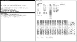
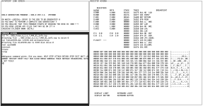
This is the dos.d_2.6_7_MAR_81_1of5.tap tape booting a Disk Pack Formatter:
It happily formats the virtual 9370 disk.

Screenshot 2024-01-10 at 18.10.00.png

The problem the is that the dos.d_2.6_7_MAR_81_2of5.tap tape fails to boot since it is not a 5500 (to little memory - tries to access code outside 16k).


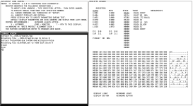
The taptim.tap is some kind of disk exerciser for the 9350 disk.

Screenshot 2024-01-10 at 18.11.04.png

Screenshot 2024-01-10 at 18.12.51.png
 

Attachments

  • Screenshot 2024-01-10 at 19.05.00.png
    Screenshot 2024-01-10 at 19.05.00.png
    19.1 KB · Views: 2
Last edited:
I have been looking at the 5500 instruction set. There are some things I haven't figured out:

There instructions like Paged Load and Paged Store that takes an LSP argument. Exactly what are they doing?

There are also "Increment and Decrement Index" instructions using LSP and MSP arguments. Cannot really figure them out.

Any input would be helpful...

I think I understood that LSP and MSP is something like Least Significant (Pointer|Part) and Most Significant (Pointer|Part) or something along those lines.

But:

With LSP you can take the MSP part from the new X register which is not present in the old 2200. But which instruction are loading anything in the X register?
I am trying to implement "Double Paged Store" DPS BC,(loc). X should point to the active page. To test that things work correctly I need to make sure that the X register is implemented correctly and that it contains something valid, but I fail to find out how X is loaded with some content!
 
While trying to understand the 5500 architecture I also hit this:

Screenshot 2024-01-11 at 17.24.56.png

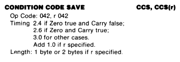
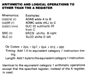
So they apparently prefix instructions starting with 2 - those are the regular register - register arithmetic and logical operations.
Then they also prefix the 0p4 which are operations normally doing same logical / arithmetics operations using immediate data.
And also a prefix for the two shift right circular ans shift left circular. Make sense.

But what is "r 0p7". There is no instruction ending in 7 except for "RETURN" which has opcode 007. The others are undefined in the 2200 instruction set.

Or am I missing something?
 
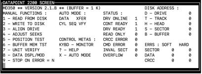
I have been trying to add 5500 support step by step and got it to the point where the DOS.D generation program starts and ask about the drive. But then it is stuck in a loop trying to format track 0 and it seems never to get out of that loop. It formats a track and then reads the same track over and over again.

Since there seem to be only one 5500 instruction (Shift Right Extended which I checked quite carefully) involved in this part of the code I expect the problem to be in how the 9370 is simulated. The information I have on the 9370 is very scarce. It is just a list of commands and registers, not how it works so it could very well be some bug in there. It can be bugs elsewhere but I think it is less likely.

Screenshot 2024-01-19 at 17.14.28.png


Code:
INFO 2024-01-19T16:13:37.816Z 10ms timeout 9370 disk read is ready on drive 0
TRACE 2024-01-19T16:13:37.819Z 0000 RETURN -> ALPHA | A=03 B=00 C=01 D=00 E=00 H=07 L=F5 C=0 Z=0 P=1 S=0 | A=00 B=00 C=00 D=00 E=00 H=00 L=00 C=0 Z=0 P=0 S=0
TRACE 2024-01-19T16:13:37.819Z 2D65 LA  4B -> ALPHA | A=4B B=00 C=01 D=00 E=00 H=07 L=F5 C=0 Z=0 P=1 S=0 | A=00 B=00 C=00 D=00 E=00 H=00 L=00 C=0 Z=0 P=0 S=0
TRACE 2024-01-19T16:13:37.819Z 2D67 DI  -> ALPHA | A=4B B=00 C=01 D=00 E=00 H=07 L=F5 C=0 Z=0 P=1 S=0 | A=00 B=00 C=00 D=00 E=00 H=00 L=00 C=0 Z=0 P=0 S=0
TRACE 2024-01-19T16:13:37.819Z 2D68 EX_ADR -> ALPHA | A=4B B=00 C=01 D=00 E=00 H=07 L=F5 C=0 Z=0 P=1 S=0 | A=00 B=00 C=00 D=00 E=00 H=00 L=00 C=0 Z=0 P=0 S=0
TRACE 2024-01-19T16:13:37.819Z 2D69 NOP -> ALPHA | A=4B B=00 C=01 D=00 E=00 H=07 L=F5 C=0 Z=0 P=1 S=0 | A=00 B=00 C=00 D=00 E=00 H=00 L=00 C=0 Z=0 P=0 S=0
TRACE 2024-01-19T16:13:37.819Z 2D6A INPUT -> ALPHA | A=01 B=00 C=01 D=00 E=00 H=07 L=F5 C=0 Z=0 P=1 S=0 | A=00 B=00 C=00 D=00 E=00 H=00 L=00 C=0 Z=0 P=0 S=0
TRACE 2024-01-19T16:13:37.819Z 2D6B XR  01 -> ALPHA | A=00 B=00 C=01 D=00 E=00 H=07 L=F5 C=0 Z=1 P=1 S=0 | A=00 B=00 C=00 D=00 E=00 H=00 L=00 C=0 Z=0 P=0 S=0
TRACE 2024-01-19T16:13:37.819Z 2D6D NDH -> ALPHA | A=00 B=00 C=01 D=00 E=00 H=07 L=F5 C=0 Z=1 P=1 S=0 | A=00 B=00 C=00 D=00 E=00 H=00 L=00 C=0 Z=0 P=0 S=0
TRACE 2024-01-19T16:13:37.819Z 2D6E SRC -> ALPHA | A=00 B=00 C=01 D=00 E=00 H=07 L=F5 C=0 Z=1 P=1 S=0 | A=00 B=00 C=00 D=00 E=00 H=00 L=00 C=0 Z=0 P=0 S=0
TRACE 2024-01-19T16:13:37.819Z 2D6F JTC 2D84 -> ALPHA | A=00 B=00 C=01 D=00 E=00 H=07 L=F5 C=0 Z=1 P=1 S=0 | A=00 B=00 C=00 D=00 E=00 H=00 L=00 C=0 Z=0 P=0 S=0
TRACE 2024-01-19T16:13:37.819Z 2D72 JFZ 2D61 -> ALPHA | A=00 B=00 C=01 D=00 E=00 H=07 L=F5 C=0 Z=1 P=1 S=0 | A=00 B=00 C=00 D=00 E=00 H=00 L=00 C=0 Z=0 P=0 S=0
TRACE 2024-01-19T16:13:37.819Z 2D75 LHA -> ALPHA | A=00 B=00 C=01 D=00 E=00 H=00 L=F5 C=0 Z=1 P=1 S=0 | A=00 B=00 C=00 D=00 E=00 H=00 L=00 C=0 Z=0 P=0 S=0
TRACE 2024-01-19T16:13:37.819Z 2D76 LAB -> ALPHA | A=00 B=00 C=01 D=00 E=00 H=00 L=F5 C=0 Z=1 P=1 S=0 | A=00 B=00 C=00 D=00 E=00 H=00 L=00 C=0 Z=0 P=0 S=0
TRACE 2024-01-19T16:13:37.819Z 2D77 SLC -> ALPHA | A=00 B=00 C=01 D=00 E=00 H=00 L=F5 C=0 Z=1 P=1 S=0 | A=00 B=00 C=00 D=00 E=00 H=00 L=00 C=0 Z=0 P=0 S=0
TRACE 2024-01-19T16:13:37.819Z 2D78 SLC -> ALPHA | A=00 B=00 C=01 D=00 E=00 H=00 L=F5 C=0 Z=1 P=1 S=0 | A=00 B=00 C=00 D=00 E=00 H=00 L=00 C=0 Z=0 P=0 S=0
TRACE 2024-01-19T16:13:37.819Z 2D79 SLC -> ALPHA | A=00 B=00 C=01 D=00 E=00 H=00 L=F5 C=0 Z=1 P=1 S=0 | A=00 B=00 C=00 D=00 E=00 H=00 L=00 C=0 Z=0 P=0 S=0
TRACE 2024-01-19T16:13:37.819Z 2D7A SLC -> ALPHA | A=00 B=00 C=01 D=00 E=00 H=00 L=F5 C=0 Z=1 P=1 S=0 | A=00 B=00 C=00 D=00 E=00 H=00 L=00 C=0 Z=0 P=0 S=0
TRACE 2024-01-19T16:13:37.819Z 2D7B EX_COM3 -> ALPHA | A=00 B=00 C=01 D=00 E=00 H=00 L=F5 C=0 Z=1 P=1 S=0 | A=00 B=00 C=00 D=00 E=00 H=00 L=00 C=0 Z=0 P=0 S=0
TRACE 2024-01-19T16:13:37.819Z 2D7C INPUT -> ALPHA | A=01 B=00 C=01 D=00 E=00 H=00 L=F5 C=0 Z=1 P=1 S=0 | A=00 B=00 C=00 D=00 E=00 H=00 L=00 C=0 Z=0 P=0 S=0
TRACE 2024-01-19T16:13:37.819Z 2D7D ND  48 -> ALPHA | A=00 B=00 C=01 D=00 E=00 H=00 L=F5 C=0 Z=1 P=1 S=0 | A=00 B=00 C=00 D=00 E=00 H=00 L=00 C=0 Z=0 P=0 S=0
TRACE 2024-01-19T16:13:37.819Z 2D7F INPUT -> ALPHA | A=01 B=00 C=01 D=00 E=00 H=00 L=F5 C=0 Z=1 P=1 S=0 | A=00 B=00 C=00 D=00 E=00 H=00 L=00 C=0 Z=0 P=0 S=0
TRACE 2024-01-19T16:13:37.819Z 2D80 RETURN -> ALPHA | A=01 B=00 C=01 D=00 E=00 H=00 L=F5 C=0 Z=1 P=1 S=0 | A=00 B=00 C=00 D=00 E=00 H=00 L=00 C=0 Z=0 P=0 S=0
TRACE 2024-01-19T16:13:37.819Z 2D4C ND  58 -> ALPHA | A=00 B=00 C=01 D=00 E=00 H=00 L=F5 C=0 Z=1 P=1 S=0 | A=00 B=00 C=00 D=00 E=00 H=00 L=00 C=0 Z=0 P=0 S=0
TRACE 2024-01-19T16:13:37.819Z 2D4E EI  -> ALPHA | A=00 B=00 C=01 D=00 E=00 H=00 L=F5 C=0 Z=1 P=1 S=0 | A=00 B=00 C=00 D=00 E=00 H=00 L=00 C=0 Z=0 P=0 S=0
TRACE 2024-01-19T16:13:37.819Z 2D4F RTZ -> ALPHA | A=00 B=00 C=01 D=00 E=00 H=00 L=F5 C=0 Z=1 P=1 S=0 | A=00 B=00 C=00 D=00 E=00 H=00 L=00 C=0 Z=0 P=0 S=0
TRACE 2024-01-19T16:13:37.819Z 027E RTC -> ALPHA | A=00 B=00 C=01 D=00 E=00 H=00 L=F5 C=0 Z=1 P=1 S=0 | A=00 B=00 C=00 D=00 E=00 H=00 L=00 C=0 Z=0 P=0 S=0
TRACE 2024-01-19T16:13:37.819Z 0280 AD  02 -> ALPHA | A=02 B=00 C=01 D=00 E=00 H=00 L=F5 C=0 Z=0 P=0 S=0 | A=00 B=00 C=00 D=00 E=00 H=00 L=00 C=0 Z=0 P=0 S=0
TRACE 2024-01-19T16:13:37.819Z 0282 LAE -> ALPHA | A=00 B=00 C=01 D=00 E=00 H=00 L=F5 C=0 Z=0 P=0 S=0 | A=00 B=00 C=00 D=00 E=00 H=00 L=00 C=0 Z=0 P=0 S=0
TRACE 2024-01-19T16:13:37.819Z 0283 ND  1F -> ALPHA | A=00 B=00 C=01 D=00 E=00 H=00 L=F5 C=0 Z=1 P=1 S=0 | A=00 B=00 C=00 D=00 E=00 H=00 L=00 C=0 Z=0 P=0 S=0
TRACE 2024-01-19T16:13:37.819Z 0285 AD  E8 -> ALPHA | A=E8 B=00 C=01 D=00 E=00 H=00 L=F5 C=0 Z=0 P=1 S=1 | A=00 B=00 C=00 D=00 E=00 H=00 L=00 C=0 Z=0 P=0 S=0
TRACE 2024-01-19T16:13:37.819Z 0287 JFC 027B -> ALPHA | A=E8 B=00 C=01 D=00 E=00 H=00 L=F5 C=0 Z=0 P=1 S=1 | A=00 B=00 C=00 D=00 E=00 H=00 L=00 C=0 Z=0 P=0 S=0
TRACE 2024-01-19T16:13:37.819Z 027B CALL 0200 -> ALPHA | A=E8 B=00 C=01 D=00 E=00 H=00 L=F5 C=0 Z=0 P=1 S=1 | A=00 B=00 C=00 D=00 E=00 H=00 L=00 C=0 Z=0 P=0 S=0
TRACE 2024-01-19T16:13:37.819Z 0200 JMP 2CCE -> ALPHA | A=E8 B=00 C=01 D=00 E=00 H=00 L=F5 C=0 Z=0 P=1 S=1 | A=00 B=00 C=00 D=00 E=00 H=00 L=00 C=0 Z=0 P=0 S=0
TRACE 2024-01-19T16:13:37.819Z 2CCE LC  01 -> ALPHA | A=E8 B=00 C=01 D=00 E=00 H=00 L=F5 C=0 Z=0 P=1 S=1 | A=00 B=00 C=00 D=00 E=00 H=00 L=00 C=0 Z=0 P=0 S=0

I find it strange that it does the read and from the disk into the buffer in the controller but never attempt to read any data from the buffer into memory (using the EX_DATA command presumably). So my impression is that there some kind of status returned that it is not happy with. I am not quite sure what it is expecting.

The flow is that it does a EX_COM3 (select disk buffer 0) and then an INPUT. INPUT normally happen after EX_STATUS, EX_DATA or EX_ADR. Not EX_COM3 unless the 9370 controller is different. Then it ANDs with 48h and directly do another INPUT ! Why? Then it RETURN from the subroutine and does another AND with 58h.

Appreciate any help it this matter! A proper document on the 9370 disk controller would be awesome!
 
Might it have to do with parity ? DP2200 IO does not know about parity, DP5500 IO does. Anyhow I have recovered the 5500 microcode ( 10 256x4 proms) , firmware ( 4 1Kx8 proms) will be done in a couple of days.
 
I don’t think it has to do with parity. There is a special instruction for input with parity. It is not used in this case. I also think that the 9370 interface is rather old so I think it is not supporting parity, but as I have very little documentation it will be hard to tell.

Very nice with the micro-code! 256 words of 40 bits, right? That is quite wide microcode for this quite simple type of machine. I am look forward adding the 5500 Boot roms to the simulator.
 
The microcode is 10 bits wide, and can also be fed from the databus in case of interrupt. Can't say I full understand it yet...
 
I think the SAMSAT people are tired/busy with people asking about Datapoint
Gordon Patterson is the guy to talk to about all things DOS. I sent you the last
email adr I have for him. He wrote big parts of it.
Unfortunately, Gordon Peterson III passed away, a year ago.
 
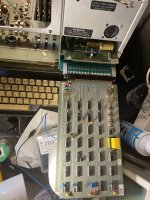
Finally I am back to the 2200 restoration. I managed to get the switch mode PSU running before the project pause. One of the reasons for the pause was that I concluded that it would be rather hazardous to work on this machine since there are live voltages coming from the PSU module in the back going to the control logic which is on a board sitting in the backplane so some signals in the backplane are live.

I thought I would hook up the machine to a regular PSU and found an old ATX PSU that I pulled out of my fathers old machine when I recapped it. The PSU also got a re-cap at the same time. The capacitors were really bad. Then I tried it. For some reason it delivered 5.8V on the 5V line. The 3.3.V was fine. Even with quite some load it still showed to high 5V. I tracked down a schematic for the control IC and the example design in there matched very well with the PSU I had. I found a resistor in the 5V sense path that had increased from 11k to 15k. Changing this one and the PSU now gave 5V out.

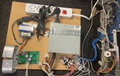
The ATX supply had +5V, -5V, +12V, -12V that was needed by the 2200 machine, but the deflection board also want to have +25V and -25V. I found a transformer that was suitable and designed a quick little linear supply. All PSU leads were connected to the DD50 connector.

IMG_3138.JPG

Now I had a PSU that could supply everything but the voltages required by the CRT so I could at least install all boards and check for some life-signs of the CPU.

But before that I wanted to make sure that the PSU filter and control circuitry board was OK. I feed voltages in it from a lab supply to check that the tantalum capacitor wouldn't short circuit. I hate when that happen. Nasty fire or spitting hot metal around.

I know that someone has worked on this machine before and while checking it for voltages my I fell on the new blue Rubycon capacitors that were installed. The probably should have been tantalum capacitors once upon a time since the rest of the +/- 12 V chain was using tantalums. But even worse, it wasn't even the right value. The schematic said 22uF / 15V while the installed blue Rubycons were 10uF / 63V. Why do people do things like this?

IMG_3137.JPG

So those got replaced with tantalum capacitors with higher capacitance.

Next step was to check the control circuitry which do the PWM control of the four big switch transistors on the PSU module. The oscilloscope told me that the signal named 14KC DRIVE had a signal that was 10.5 kHz.

I then connected the 60V SENSE input signal to a lab power supply. At first the frequency increased to around 28 kHz and when getting close to 60V (which is the target voltage of the first buck converter) the frequency got lower again. Perhaps this is how the regulation should work? Not really a PWM signal that I would expect with constant frequency and varying pulse width.

Next step is to start testing with boards installed. First the CPU and then the rest one by one.
 
Installed the boards one by one and eventually all boarfs except the memory boards were in it. It consumed around 7.5A on the 5V. No smoke. No exploding tantalum capacitors.

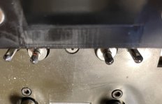
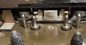
At power up the two LEDs marked SYNC and INT was lit. Installing a random cassette tape in the rear drive and pressing RESTART button started the drive in forward direction and the two LEDs went out. Pressing STOP momentarily stopped tape motion. The same if I pressed RESTART again. The other keys didn’t do anything.

According to the manual pressing RESTART should rewind the tape and then start forward motion. But the rewind never happened when I pressed RESTART.

Unfortunately it is really hard to measure on the processor board without extender boards so it is really hard to tell if the machine is doing the right thing at all.

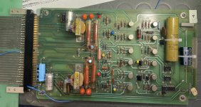
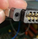
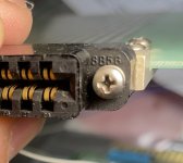
Anyone that knows what connector they used?

IMG_3144.jpeg

IMG_3142.jpeg

IMG_3143.jpeg

It looks like the Litton Industries logo. The pitch is 0.156 inch or 3.96 mm. But where the keying is located the distance is just 7 mm rather than expected 8 mm.
 
If cassettes are giving you trouble then there is the option to replicate the ROM boot board : an easy way to get a simple monitor running in your machine.
 

Attachments

  • Boot_ldr.pdf
    72.2 KB · Views: 0
Yes. I know. I will create a breadboard as well as extender boards so that I can measure more easily. The breadboard can then replace the demodulator board and include a STM32 uController that simulates the tape.

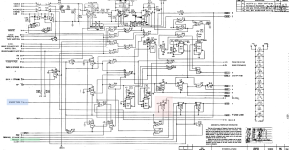
It is really hard to tell if the machine is doing the right thing. The RESTART button goes through two inverters and then to the preset input of the INT and SYNC flip-flops. Those go inactive when pressing the RESTART button in the correct way. But other than that it is difficult to trace the operation of the RESTART signal… Hence the need for extender boards.
 
Back
Top