• Please review our updated Terms and Rules here

PDP-11 style front card

tech58761

Experienced Member
Joined
Nov 10, 2023
Messages
57
Location
Northern Plains, USA
I spoke a while back about two PDP-11 systems in a room next to my current work area. So far, I haven't heard anything about any long-term plans for these (we have plenty of space now and these two machines are well out of the way of the main production area). However, it looks like my area will be moved back into the main building within the next few weeks.

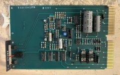
I had a moment and took a look at the 'spare' chassis I mentioned in my previous thread and realized the 'front panel' board was actually loose in the rack, Looking at it, I realized that it was actually one of the equipment manufacturer's boards, and a quick search on the board number turned up almost nothing useful. So, I plan to make a BOM and node list for this board so I can draw and share the schematic. Looks like it uses a literal handful of lines besides the usual +5 / +12 / ground connections.
 

Attachments

  • card.jpg
    card.jpg
    283.3 KB · Views: 52
It looks like the logic to produce the handful of QBUS signals to make a PDP-11 'work'. This logic is usually on a separate board and within the DEC PSU.

Part of it will implement the power on sequencing.

It looks like these circuits have been put on a single dual-height QBUS card rather than being spread to the four winds.

If this is the case, this would be quite a nice card to have available.

It would also mean that you could use any manufacturer's power supply for the PDP-11.

Dave
 
daver2: I figured it would be worth documenting for the community. I have a working BOM completed and a list of component pins ready to start compiling into a node list for a schematic.

The board has "PWR SEQ 2" on it, and if I understand the Qbus slot numbering scheme correctly, these are the specific pins used by the board:

Left: F1, J1, M1, P1, T1, A2, C2, D2
Right: A1, B1, E1, H1, J1, M1, R1, T1, V1, A2, C2, D2
 
According to my notes, and assuming that by "left" you mean the edge-connector by the axial electrolytic caps -- thus the "A" position, then:

Left: SSpare2, GND, MSpareA, BHALT, GND, +5, GND, +12
Right: BDCOK, BPOK, BDAL20, SSpare8, GND, GND, BEVNT, GND, +5, GND, +12

Some inexplicable assignments in there ...
 
So, which ones are the unexpected pins?

I'm also puzzled about the presence of a 7805 and a 7912 regulator on the board.

It seems the 5V bus on the board is fed from the 7805.

The two metal cans appear to be 2N5433 JFETs, but I'm only seeing 8 ohms from drain to source?
 
Last edited:
It is likely that the logic on the board will require its own power supply that is independent of the QBUS supplies themselves. After all, this may well be a power up sequencer...

Is it possible that the 'spare' signals are separate power rails for the logic on this card? Perhaps follow these spare signals back onto the QBUS.

Dave
 
I guess it does make sense to derive the +5 from a 'bulk' supply before giving the go-ahead to the main P/S to activate the 5V supply.

BDAL20 goes to the group of four 1N4002s near the edge connectors.
 
For reference I've attached documents for the H780 power supply that is used with the 4-row 11/03 chassis (BA11-ME). I would expect some similarities between what you're reverse-engineering and what DEC designed as they serve the same purpose.
 

Attachments

  • H780 Power Supply.pdf
    256.7 KB · Views: 3
  • H780 FMPS.pdf
    1.4 MB · Views: 2
There are two test points - the BEVNT pad goes to the point marked 'B' and nowhere else. Is it intended to be jumpered to A during testing? Test point 'A' goes to pin 3 on the 7438.
 
I guess it does make sense to derive the +5 from a 'bulk' supply before giving the go-ahead to the main P/S to activate the 5V supply.

BDAL20 goes to the group of four 1N4002s near the edge connectors.
Probably stepped-down line voltage to generate the LTC. I'm guessing the LM339 is used as well in the LTC circuit...
 
The LM339 gets power from the 7912, and it looks like both the bulk power for the 7805 and 7912 pass through those seven 1N4002s, so low-voltage AC is definitely plausible, especially if only a few dozen milliamps are needed.

Currently well into the node list - started with ~270 component pins to document, and have about half that at this point.
 
Completed the node list, now starting to draw the schematic. I find it interesting that all the TTL gates are the open-collector style ('06 vs '04, '09 vs '08, '38 vs '00).

Also a '14 Schmitt Trigger and two '122 multivibrators. On the analog side, there's an LM339 and an LM393 (I assume this is the 2-unit version of the LM339).
 
Posting an in-progress shot of the schematic in case there's anything odd that I need to double-check.

When the schematic is drawn and neatened up, I'll post the actual KiCad schematic file.
 

Attachments

  • IN PROGRESS.pdf
    184.2 KB · Views: 17
Back
Top