• Please review our updated Terms and Rules here

PDP-11 style front card

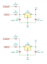
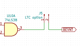
IMO it would be better to label the pins by their logical designation rather than by their physical ID. For example, meaningless "right 14a" which you have connected to "J4". I expect that the LM393 circuit is generating the LTC, being fed from an AC source on "right 14a", and being optionally connected to the backplane BEVNT via "J3" -- see the specification for this signal on http://web.frainresearch.org:8080/projects/pdp-11/q-bus.php. BE1 thus should be labeled "SSpare6" (Special Spare 6) and evidently is an AC input.

Similarly "left AP1" is BHALT and the debounce circuit around the Halt switch also then makes sense.

At the moment I'm assuming that all power rails are being supplied from the backplane and the two on-board regulators are uninvolved.

"right 7a / BH1" should be labeled "SSpare 8" (Special Spare 8) and is TBD as to function at this stage. In effect it's being ANDed with an AC signal that we inferred on BE1 and then being thresholded as in the case of the LTC circuit, driving a pulse generator that's going to be significant on both the rising and falling edges judging by the downstream circuitry. Three RC delays are implemented. Looking forward to seeing BDCOK and BPOK connected :->.

Perhaps "SSpare 8" comes from an external AC power switch or power fail sensor?
 
There are two test points - the BEVNT pad goes to the point marked 'B' and nowhere else. Is it intended to be jumpered to A during testing? Test point 'A' goes to pin 3 on the 7438.
It appears that this jumper *optionally* feeds the LTC onto the BEVNT signal line. Remember that there could be an alternative LTC (or other clock source) implementation on the backplane so this isn't really a test point; it's a configuration choice which would be a wire-wrapped connection. In your case the LTC isn't being used. Which implies that *potentially* "SSpare6" isn't furnishing an AC signal-input to any circuit, and specifically the power-OK circuit, which might explain the presence of the other input there. Hypotheses proliferate :->.
 
Good information thus far - based on the feedback on the test points, the attachment shows how I reworked that section:

I have about half the nodes left to input. It definitely looks like a small AC source is being fed to this board through the backplane to feed the +5 and -12 regulators.

One thing I JUST noticed is that the glue logic is straight 7400 (will correct that in the schematic momentarily) - there is only one LS chip. I don't know if that matters regarding propagation delay.
 

Attachments

  • Screenshot 2024-02-18 at 8.13.47 AM.png
    Screenshot 2024-02-18 at 8.13.47 AM.png
    8.3 KB · Views: 3
if you are changing TTL families, just beware of a potential latent design error with the original. Read: https://www.ti.com/lit/an/sdya009c/sdya009c.pdf.

You can directly connect the input of a 74LS series device to +5V without a pull-up resistor.

However, do not do the same thing for a 74 series device. Use a pull-up resistor.

I noticed there were some pins like this on U4 (pins 4 and 5). If this is a 74LS122 - all is good. If it now is a 74122 - you really require a pull-up resistor. The TI document contains the equation to calculate the value of the pull-up resistor. The resistor can be shared with other inputs.

Dave
 
I still have about 20 resistors left to add into the schematic; at this point the intent is to document what is there. :)

We can hash out any 'best practice' updates once I have everything drawn out.

Also, here's detail on the two on-board regulators:
 

Attachments

  • Screenshot 2024-02-18 at 8.58.48 AM.png
    Screenshot 2024-02-18 at 8.58.48 AM.png
    14.4 KB · Views: 6
>>> We can hash out any 'best practice' updates once I have everything drawn out.

Exactly. Just wanted to make you aware of my first thought...

That looks sensible for the regulators though.

My gut feeling is that the external transformer connected to SSpare8 and BDAL20 (although the SSpare6 id would be better in this case) is centre-tapped with the centre-tap being connected to 0V. Obviously, this is outside of the card, but you would need to check this out later.

Dave
 
I'll see what I can do regarding getting access to that spare rack long enough to go prying into the P/S.

Okay, here we go! Got the last of it inputted and it passes KiCAD's ERC check. If it looks good I'll neaten it up and upload the schematic file.

Three black tubular parts (R5, R14, R43) I thought were resistors across +5 and ground, I now assume are 0.01uF bypass caps and renumbered them accordingly to C12-C14.
 

Attachments

  • proofread.pdf
    214.6 KB · Views: 6
Last edited:
My gut feeling is that the external transformer connected to SSpare8 and BDAL20 (although the SSpare6 id would be better in this case) is centre-tapped with the centre-tap being connected to 0V.
Doesn't take much "gut" to make that call :->. So the dual input to the power signal circuitry picks off both halves of the AC cycle as input, not just one.

When we get to the point of evaluating the RC timing parameters, here's the relevant portion of the Qbus specification for reference. Looking forward to seeing which ICs/circuitry the onboard regulators are supplying ...
 

Attachments

  • Q-bus Power Up-Down Protocol (EL-00160-00-0_A_DEC_STD_160 Sep91).pdf
    86.2 KB · Views: 3
pbirkel: In this case, the +5 regulator supplied the TTL logic and one side of the LM339 supply, and the -12V regulator supplied the negative side of the LM339 supply.

I've posted the schematic just above.
 
>>> Doesn't take much "gut" to make that call :->.

Always throw a bit of doubt into there until it is checked out for sure!

Dave
 
pbirkel: In this case, the +5 regulator supplied the TTL logic and one side of the LM339 supply, and the -12V regulator supplied the negative side of the LM339 supply.

I've posted the schematic just above.
OK, so for clarity then I'd label the edge-connector "+12" to "+12VA" akin to the "+5VA" to make clear that both are the monitored rails, distinct from the internal power rails. And I'd remove the "PWR_FLAG" indicators from both since they are really only signal lines in this circuitry, not distributed power.

And of course I'd change the labeling of "BDAL20" :->.
 
I'll see what I can do regarding getting access to that spare rack long enough to go prying into the P/S.
if you do, see whether there are any markings on the transformer that supplies those two pins. 20-or-more VAC C.T. I'd think would be sufficient to meet the requirements of the LM7912. Probably a low-cost 24 VAC C.T. transformer of modest power rating, if it's stand-alone ... which I assume if it's going to be always-on.
 
>>> And of course I'd change the labeling of "BDAL20" :->.

And add a government health warning to the schematic to make it clear that this card will NOT work in a 22bit system. Otherwise BANG!

I wonder if this could be part of the 'enhancement'? Use the 'spares' available on a 22 bit system instead...

Dave
 
I've swapped the 12V labels, and the PWR_Flag is just there to satisfy KiCAD's ERC (Electrical rules check) function. I can drop those symbols before uploading the schematic.

What would you suggest for a replacement mnemonic for BDAL20?

Once we're all on the same page as to function, I'd be glad to make a separate version where we can add in 'best practice' changes.

Since this apparently replaces the functions specific to the DEC supply, we could make it more universal...
 
As per my post above "... and BDAL20 (although the SSpare6 ID would be better in this case) ...".

SSpare6 was the original QBUS connector name before the 22-bit backplane came along.

Dave
 
...PWR_Flag is just there to satisfy KiCAD's ERC (Electrical rules check) function.
Only if that is truly a power rail and thus should not be visible as lines all over the schematic. In this case it's really a signal and should be traced out with a visible line, like other signals. Which would make the working of the circuitry in that regard even clearer. IMO :->.
 
Only if that is truly a power rail and thus should not be visible as lines all over the schematic. In this case it's really a signal and should be traced out with a visible line, like other signals. Which would make the working of the circuitry in that regard even clearer. IMO :->.
I *would* add a label to each signal line indicating what that signal is termed on the backplane.
 
This board is a part of a Universal Instruments 8222 machine controller which is an LSI11 based 18bit QBUS chassis.
Here are some informations about this board as well as about the 8222 machine controller.

// Peter
 

Attachments

  • 8222 slide show.pdf
    946.9 KB · Views: 11
  • 41273401-01.png
    41273401-01.png
    524.5 KB · Views: 13
  • 41273401-02.png
    41273401-02.png
    331.4 KB · Views: 13
Back
Top