• Please review our updated Terms and Rules here

PETunia's Repair Log

His Dwight,
Excellent tutorial. I forgot that simple voltmeters only rectify AC signals to drive the meter movement. On my VOM there is an 'Out' jack in addition to the '+' and '-' jacks. Does that jack insert a capacitor in the circuit? Can that be used to remove DC bias voltage?

I've not see such, that I remember, on a VOM. It is much easier to just get a capacitor. They are not all to uncommon. I'd send you one but it isn't worth the postage.
Dwight
 
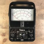
After a little searching, I get to instruct Dwight on the operation of a Simpson VOM! (Blushing with pride) :p

Here is a blurb from the manual:

4.14 Output Voltage Measurement
It is often desired to measure the AC component of an Output Voltage where both AC and DC voltage levels exist. This occurs primarily in amplifier circuits. The 260-8 has a 0.1 mfd, 400 volt capacitor in series with the OUTPUT jack. The capacitor blocks the DC component of the current in the test circuit, but allows the AC or desired component to pass on to the indicating instrument circuit. The blocking capacitor may alter the AC response at low frequencies but is usually ignored at audio frequencies (Figure 4-8 ).

otsrif1jm1ny08a101ew.jpg
 
I've been out of circulation for a few days (good things not bad) so unable to take things much further... until yesterday...

Firstly I tried out a 8K RAM replacement board I have been thinking about but that didn't go well (probably should wait until I have a working PET) and created quite a lot of snow on the screen so I thought the address decoding perhaps was not working as expected... anyway I abandoned that project for now and started scoping some traces... I was particularly interested in /SEL0, /SEL1, BA10 and BA11 to explain my snow... anyway..

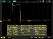
I scoped a few pins... and although this may or may not be relevant I got a trace on BA10 which really doesn't look healthy...

BA10.jpg

Moving back to Pin 19 on the 6502 I get...

6502_A10.jpg

which looks a lot more healthy.

Now the only thing between BA10 and A10 is the quad inverter at E4... so either that isn't driving hard enough or there is a problem on the BA10 side????

I removed all RAM, both PIAs, all ROM and except a 2716 containing the vossi PET tester and it starts OK but the BA10 signal is as above.

For comparison...

BA11

BA11.jpg

PS
I'm still a bit concerned about the power supply stability... will scope the big blue cap next time.
 
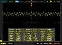
It's been nagging me so I scoped across GND and the RED side of the Big Blue Capacitor

PSU_Across_Big_Blue.jpg

There is 480mV ripple but the minimum, 9.2V, is way above where the Voltage Regulators should care? It's around 100Hz... 2x mains?
 
If it is the capacitor I am thinking about, this capacitor is before the voltage regulators. There will be about 9 Volts or so here. You are in the UK (so 50 Hz mains supply) full-wave rectified will give you a small sawtooth at 100 Hz (as you have found).

Providing the output from the regulators are all +5 Volts +/- 5% (+/- 0.25 Volts = 4.75 to 5.25 Volts) you are ok.

The signal on BA10 looks better than I have seen on some working PETs... it looks a bit slooow on the 0 to 1 transition, but that is sometimes what you see.

Dave
 
There is 480mV ripple but the minimum, 9.2V, is way above where the Voltage Regulators should care? It's around 100Hz... 2x mains?

As Dwight said in his message, 50 Hz would indicate a bad rectifier and a large 100 Hz ripple may indicate a failing filter cap. My reading at that point was 125 mV of ripple. Measure the ripple on the regulator outputs. Mine read only a few mV.
 
Thanks for the confirmation of the 9V... think I can rule that out for the time being.

So I did something else I should have done before... clocks...

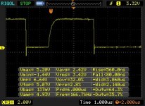
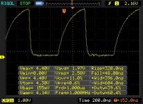
First 6502 Pin 37 (phi0 clock in)...

6502_Pin37.jpg

looks nice and square...

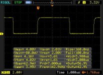
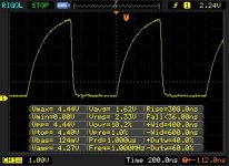
Then Pin 39 (phi2)...

6502_Pin39.jpg

Sharks! I didn't expect that

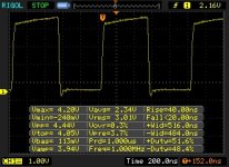
phi2 goes into a 2-input NAND acting as an inverter... and then another one... at the output of the 1st pin 11 G3...

G3_Pin11.jpg

So a lot squarer than the sharks and this is the signal the RAMs and ROMs see... whereas the PIAx2 and VIA see sharks. (PIAx2 and VIA currently removed so little hanging off phi2)

I have nothing to compare this to but the phi2 looks too non-square?

I guess I should replace the 6502??? but I don't have any spares... where is a reputable source for a 6502? (I normally buy most of my components from Farnell since I am UK based; I am a bit wary of ebay due to fakes).
 
The signal on BA10 looks better than I have seen on some working PETs... it looks a bit slooow on the 0 to 1 transition, but that is sometimes what you see.
That's good to know. I slightly misread the schematic... BA10 goes through a buffer E4 (7417), whereas BA11 goes though a pair of inverters E5 (74LS04) so I guess the shape might vary.
 
After a little searching, I get to instruct Dwight on the operation of a Simpson VOM! (Blushing with pride) :p

Here is a blurb from the manual:

4.14 Output Voltage Measurement
It is often desired to measure the AC component of an Output Voltage where both AC and DC voltage levels exist. This occurs primarily in amplifier circuits. The 260-8 has a 0.1 mfd, 400 volt capacitor in series with the OUTPUT jack. The capacitor blocks the DC component of the current in the test circuit, but allows the AC or desired component to pass on to the indicating instrument circuit. The blocking capacitor may alter the AC response at low frequencies but is usually ignored at audio frequencies (Figure 4-8 ).

View attachment 62441

Good old Simpson. I have two around the house someplace. I should have looked.
I'll admit I recall looking at the inside a long time ago and thought it was some form of DC isolation. It was clearly lost in the pile of cells at the top of my body.
Thanks Dave.
Dwight
 
That's good to know. I slightly misread the schematic... BA10 goes through a buffer E4 (7417), whereas BA11 goes though a pair of inverters E5 (74LS04) so I guess the shape might vary.

Most TTL have very asymmetric currents for 1 to 0 than 0 to 1. The pullup is about 10:1 or more. Bus buffers are often closer to 1:1. An unloaded output will show an almost square wave but a high capacitive load will show this more clearly. The 74LS04 has 0.4ma pullup and 8ma pulldown, 20:1.
This is why, many circuits use the falling edges for timing, such as disk drives and chip selects, even 74138 or 74139.
Dwight
 
Well I managed to find a R6502AP in my hoard so I swapped that and...

Same Sharks

6502B_PHI2.jpg

So I guess that is how it is and as pointed out the negative edge is well defined and the squared up version at the output of G3 at pin 11 looks nice enough.

Might have to rethink my strategy
 
Don't get discouraged. This is what trouble shooting is all about. You have a hypothesis as to what the problem might be and then you prove it either true or false. I need to go back through the previous post to see what we've looked at so far. Also, information gathered along the way helps to isolate the problem better.
Did you do the ripple measurement of the 5v with a method you trust? I guess 700+ millivolts would show on a scope clear enough.
Dwight
 
I lose track but the power supply ripple seems manageable on all Voltage Regulators... i did measure recently but need to improve my note keeping.

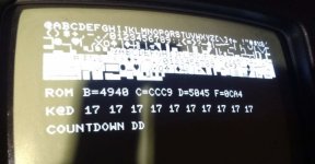
I have more inconsistent behaviour now... the ROM checksums are changing using both versions of the tester. I'm trying to establish the exact circumstances of that but it suggests there is bus contention. It's very weird because the testers suggest the ROMS and RAM are OK some of the time...

I'll report back
 
We seem to be ‘flipping’ from one thing to another without actually chasing down any actual problem.

The common theme seems to be power supply. So, as Dwight has suggested, let’s run this to ground first.

Second, put my PETTESTER ROM in place of the EDIT socket and let’s get as much information from that before moving on. For example, we never got to the bottom of the kernal ROM ($Fxxx) checksum being wrong. Either my documentation is incorrect, or you may have a bad ROM somewhere. Put at least 4K of RAM in the machine and run the RAM test for a good half a day.

We can then reconvene with some hard data to work with.

Edit: Our posts crossed. Your behaviour could be indicative of power supply, faulty components, bad connections or environmental issues (e.g. temperature or EMC effects). A NOP generator can help identify bus contention and I can write specific test software to help isolate a fault if necessary.

Dave
 
re: Checksums...

I think that was... F=0CA4

Checksums.JPG

I think that is OK....

hxd.JPG

assuming that rom-1-f000.901439-04.bin and rom-1-f800.901439-07.bin are appropriate images.
 
re: PSU

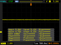
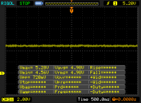
Voltage Regulators are around 5V with Vpp 560mV, 720mV, 640mV and 720mV.. traces...

VR1
VR1.png

VR2
VR2.png

VR3
VR3.png

VR4
VR4.png

and across Big Blue Filter CAP..

PSU_Across_Big_Blue.jpg

I'm pretty sure that although not perfect it is probably all good enough
 
re: Latest theory... bus contention due to incorrect logic decoding...

I have always got inconsistent results and seemingly these are more inconsistent with RAM in the machine so I have a theory that there is contention somewhere...

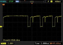
I did find something nasty looking on pin 19 of H8 & H9... which is the output of G3 pin 6... (looks a bit like a herd of elephants going leftwards)

G3pin6.jpg

the respective inputs are...

G3 pin 4...

G3p4.jpg

and

G3 pin 5

G3p5.jpg

Maybe another random chicken move... not sure...

PS
Sadly I only have a 2CH scope otherwise I would probe pins 4,5 and 6 of G3 simultaneously
 
Last edited:
Can Dave or someone tell me which schematic I should be looking at. I'd like to suggest a few things to look at?
Dwight
 
Back
Top