• Please review our updated Terms and Rules here

Plugging in power to other side..

falter

Veteran Member
Joined
Jan 22, 2011
Messages
6,580
Location
Vancouver, BC
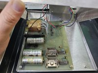
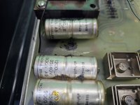
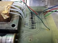
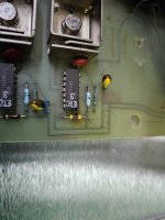
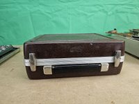
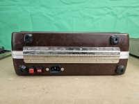
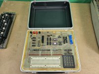
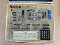
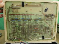
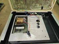
Silly question.. I have a homebrew MMD-1 I'm taking an interest in again. It has its own PSU but the PSU isn't cranking out enough volts. I want to bypass it for now and work on the board. My question is this - the three voltage leads from the psu are soldered to the backside of posts that the user can connect stuff to on the top side of the board. If I just connect a working on the top side is it possible for something to go wrong with the old psu still connected but not plugged in? Or do I need to remove the wires from that psu, from the back first
 
Well, I don't know what a MMD-1 is, but I recommend that you install a connector between the board and the PSU. I wouldn't recommend back-feeding with the old PSU connected.
 
You can probably leave the 0V/GND wire connected and just disconnect the actual power voltage power rails from the PSU to the MMD-1, but this doesn't (in my mind) make sense to me.

Dave
 
Thanks guys. Yeah I figured but just wanted to check. I'll desolder the wires. This is the machine I'm talking about, aka the Dyna-Micro by Jon Titus. This one appears to be homebrewed.. it has the later MMD-1 PCB design but someone etched the board themselves and did some mods, and then installed it in a briefcase. It had a different crystal than the MMD1 has (I think the MMD1 has a 6.something mhz). I tried swapping parts years ago and tried with both original and 'correct' crystal but never could get it to run right. Have a feeling the mods have something to do with it.
 

Attachments

  • 20231027_162707.jpg
    20231027_162707.jpg
    3.8 MB · Views: 27
  • 20231027_162714.jpg
    20231027_162714.jpg
    3.8 MB · Views: 33
  • 20231027_162733.jpg
    20231027_162733.jpg
    4.3 MB · Views: 47
  • 20231027_162740.jpg
    20231027_162740.jpg
    4.4 MB · Views: 47
  • 20231027_162750.jpg
    20231027_162750.jpg
    4.4 MB · Views: 45
  • 20231027_162752.jpg
    20231027_162752.jpg
    3.6 MB · Views: 35
  • Screenshot_20231027_163824_Adobe Acrobat.jpg
    Screenshot_20231027_163824_Adobe Acrobat.jpg
    422.7 KB · Views: 30
A 6 millihertz crystal is a very slow clock rate. Did you wait for an hour to see if it reset :)? Sorry, I couldn't resist...

We should be able to work out what is going on with a multimeter and oscilloscope. This should not be that tricky a job (unlike your pesky tennis game)!

What is actually wrong with your power supply - before you start doing circuit surgery. There cannot be much to this to debug either.

Dave
 
So,

GND = Black terminal = Black wire.
+5V = Red terminal = Green wire.
+12V = Red terminal = Red wire.
-12V = Black terminal = Blue wire.

So what does each supply read (referenced to 0V/GND = Black terminal = Black wire)?

Dave
 
A 6 millihertz crystal is a very slow clock rate. Did you wait for an hour to see if it reset :)? Sorry, I couldn't resist...

We should be able to work out what is going on with a multimeter and oscilloscope. This should not be that tricky a job (unlike your pesky tennis game)!

What is actually wrong with your power supply - before you start doing circuit surgery. There cannot be much to this to debug either.

Dave
The power output seems to be flaky on the PSU. On the +5v when you turn on it hits 3.5v and then drops to 1.5v. Nothing on the +12 or -12v rails. It was working before. The power button is one of those press once and it locks, press again to release designs.. the lock has failed so I have to jam a piece of paper in between the button and casing to hold it down.
 
Most PSU's SMPS types at the final output use diodes to charge the output filter caps. This means that if you did have two PSU's where the outputs were connected together, and one psu was switched off, all that would happen is, that in the psu that was turned off, its output filter caps would get charged, but its diodes would get reverse biased and it is not a problem.

However for an analog supply with a series pass regulator it is a different cup of tea. In a type where the emitter of the pass transistor is the output and you back feed it when it is powered off, the B-E junction can reverse break down. In Analog regulators, like LM317's etc or other linear regulators, it is recommended to place a diode backwards across the regulator output to its input to prevent this problem causing damage to the pass transistor if the output of the supply gets powered by another source when it is turned off.
 
It looks like we may have two (2) ICs missing?

One looks to drive some of the LED's.

The two yellow wires on the component side look a bit suspect to me (where they go to the 7475 LED driver on the lower left).

This will not be the cause of the PSU problem though.

Can you point us to the schematics for the 'base' variant of this machine at all?

Dave
 
Sorry I should have mentioned those pics were just after I pulled it from the shelf. The correct parts have since been installed.

The original Dyna Micro was covered in May and June 1976 editions of Radio Electronics (May here). What I don't know is how much changed between the original product and the production MMD-1 that was sold to educational markets. One obvious difference is they removed the edge connector and switched to a ribbon cable style. But what else they changed if anything I'm not sure. I think the original schematic is basically same.
 
Just found them.

https://www.worldradiohistory.com/Archive-Radio-Electronics/70s/1976/Radio-Electronics-1976-05.pdf - page 33 onwards.

https://www.worldradiohistory.com/Archive-Radio-Electronics/70s/1976/Radio-Electronics-1976-06.pdf - page 41 onwards.

https://www.worldradiohistory.com/Archive-Radio-Electronics/70s/1976/Radio-Electronics-1976-07.pdf - page 48 onwards.

There is probably not much that has changed - but having the original schematics and PCB layout means that we can check.

Your layout looks pretty much the same (although I have noticed another missing IC on yours now I come to do a "spot the difference"...

As you say, there are a load of modifications to your board.

There is no schematic for the power supply in the article though. From the photograph it just looks like conventional series-mode voltage regulators. Is it possible to remove the 'lid' from the PSU and get some photographs?

It looks like the 7805 (the +5V regulator) is the thing with insulation tape around it bolted to the lid. The black lead will be 0V/GND, the green lead to the 7805 regulator will be the input and the red lead from the 7805 will be the output. If you can, measure the voltage going into the 7805 regulator on the green lead (relative to the black lead). Note that the insulating tape is to prevent the leads shorting out against the case!

Dave
 
Last edited:
Your machine is fully expanded.

I notice that there is no crystal. That is what the yellow wires were for...

You say you have a 'strange' crystal on your machine. So what have you got, and where is it soldered to?

The original crystal was 6.750 MHz.

Perhaps a photograph of the board as you have it now would help?

Dave
 
A very interesting early trainer for hobbyists and educators designed by John Titus. Absolutely loving that suitcase enclosure - I bet when the maker walked into the room with that baby, you could smell the nerd on him :)

I would remove/isolate the PS and test it under appropriate loads first. There could be multiple possibilities for "The power output seems to be flaky on the PSU. On the +5v when you turn on it hits 3.5v and then drops to 1.5v. Nothing on the +12 or -12v rails."
If you can manage it, a trip to this museum (note that it moved) with it might get you an expert opinion...

 
By doing a very quick comparison against the PCB foils in the manual and your photographs I have concluded that your machine has NOT been heavily modified from the original.

It would appear as though the 'home-brew' PCB has some missing PCB tracks - these have been rectified by adding some of the wires.

The other wires seem to be associated with PCB tracks that are there - but they are (or should be) through-hole plated to tracks on the component side. For some reason, I suspect that these were not making contact, and have also been replaced by wires.

I agree with disconnecting the power supply and rejuvenating it separately.

Ah, things are flooding back. The 1702 EPROM requires -9V, and this is generated on-board from the -12V supply. We definitely require the +5V and -12V to be working to get any sign of sanity from this machine. And (of course) the CPU and clock requires the +12V supply - so we basically have to 'fix' the PSU one way or another before we can start work on the PCB...

And -5V (for the CPU) is also generated from the -12V supply.

Dave
 
Last edited:
The schematic is fairly straight-forward. Perhaps (before powering up the PCB) we should check things out 'by eye' and with a multimeter. There are a lot of things we can check to ensure we have continuity between where we expect to. This will at least minimise faulty wiring and PCB tracking (especially through-hole interconnections).

Once we have the PSU working - we can make some significant inroads with a multimeter and oscilloscope.

Dave
 
I think I can account for most (if not all) of the wires now.

Most of them are definitely where the PCB tracking is missing (or otherwise damaged). However, the keypad that has been used looks completely different to the original - hence the major wiring around this area.

Dave
 
You can check that the keys work as follows (with the power OFF):

Check from IC5 (8224) pin 2 to +5V rail that the resistance is approximately 1 kOhm.

Check from IC5 (8224) pin 2 to 0V/GND that the resistance is quite high. Press the reset 'R' key on the keypad, the resistance should fall to a very low value.

You can also check that the remaining keys on the keypad work by measuring the resistance from the inputs of IC32 and IC33 (74148) between each input pin and 0V/GND are high until the associated key is pressed on the keypad. Look at the schematic (FIG. 2 of the magazine article) for the association between the keypad keys and the input pins of the ICs.

I would always measure the resistance directly on the pin of the IC - and try not to push too hard. This is to ensure that the IC pin is in good contact with the IC socket. Too much force may inadvertently cause a poorly connected IC pin to make a better contact with the IC socket.

I think that is all the testing you can really do (without power at least) apart from perform continuity tests between all of the various pins of the ICs following the schematic. Use a highlighting marker to mark each off on a paper copy of the schematics as you test each pin.

Note that there are 2 extra RAMS and 1 extra PROM on your board. In general, the address, data and power pins should all be wired in parallel between the ICs of the same type. This is true EXCEPT for the chip select lines. In the case of the EPROM this is pin 14 and in the case of the RAMs this is pin 15.

These corresponding pins on the extra RAM and EPROM should be wired to the address decoder IC14 (74LS155) pin 12 (for the extra EPROM) and pin 5 (for the extra RAM).

Dave
 
Last edited:
Here are pics of the PSU board as best as I can get them. One of the resistors looks a bit scorched.

The crystal I tried to use this with (which is not present in the photos but I have attached now) is 6750khz. I am having trouble locating the one that was there before but I want to say it was faster.. like 10000khz+. Have to dig for photos.
 

Attachments

  • 20231028_090354.jpg
    20231028_090354.jpg
    3.7 MB · Views: 35
  • 20231028_090350.jpg
    20231028_090350.jpg
    3.2 MB · Views: 33
  • 20231028_090347.jpg
    20231028_090347.jpg
    3.2 MB · Views: 31
  • 20231028_090342.jpg
    20231028_090342.jpg
    1.5 MB · Views: 33
Back
Top