• Please review our updated Terms and Rules here

Project to create an ATX 80286 mainboard based on the IBM 5170

Thanks a lot lowen for this additional info, it's more clear now and super useful!

From the important fact of active production and since I am starting a new design I think it would be a good idea to choose an Atmel part and go for the method of converting the output file and using the ATDH1150USB.

When I started to look at these chips I didn't know about the differences so thanks, that's important.

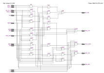
After trying out Quartus 11 I could see after everything is assigned to the package that there are only 10 pins free now. Only few macrocells are needed. So if I want more I could indeed perhaps look at a larger chip like the ATF1508 which you linked to. This chip has a lot more pins available. I will probably order the ATF1508 and ATF1504 because I am not sure how much I will want to integrate, this also depends on test results.

I will try to find Quartus II 13.0 SP1 as you mentioned since this is newer than 11.

I have read that some of the pins can be freed if I choose not to be able to use JTAG after programming however that's not practical during development when I need to program and compare and program again each time. I could also develop using the ATF1508 and then evaluate after everything is 100% functional which chip will be the best choice on the PCB.

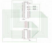
Quartus is really great to use and super elaborate, though I still need to get the procedure right of setting up a project, I was successful already to get further to be able to create the programming files(including a .POF file) of my intermediate test version of the logic.

It's pretty amazing to see how fast Quartus can break down the schematic and to see it redrawn in netlist view, and to see how it can sort out the equations in a really ordered way in the equation file. I am starting to see the huge advantages there.

I will order the ATDH1150USB and a few parts tomorrow so I can quickly get started, your advice is much appreciated, thanks!
 
Here is a diagram by Quartus using the netlist viewer.
My original schematic is maybe twice larger in size.

And here are the new equations generated from it, which is not the complete logic yet for replacing U87, but after I receive the parts needed I will proceed to get the complete logic. Maybe studying this reduction logic can inspire me how IBM designed the original part.

Code:
--A1L18 is inst~2
A1L18_p1_out = /AEN_1 & /AEN_2;
A1L18_or_out = A1L18_p1_out;
A1L18 = A1L18_or_out;


--A1L17 is inst30~9
A1L17_p1_out = Q1 & !/IO_CS_16 & AIOW;
A1L17_p2_out = Q1 & !/IO_CS_16 & !/IOR;
A1L17_p3_out = RAS & !/RES_0WS;
A1L17_p4_out = AIOW & !/RES_0WS;
A1L17_or_out = Q4 # A1L17_p1_out # A1L17_p2_out # A1L17_p3_out # A1L17_p4_out;
A1L17 = A1L17_or_out;


--A1L15 is inst20~7
A1L15_p1_out = RAS & !FSYS_16 & XA0 & /AEN_1 & /AEN_2 & !XBHE;
A1L15_p2_out = !FSYS_16 & XA0 & /AEN_1 & /AEN_2 & !XBHE & !/MEMW;
A1L15_p3_out = XA0 & /AEN_1 & /AEN_2 & !XBHE & AIOW & /IO_CS_16;
A1L15_p4_out = XA0 & /AEN_1 & /AEN_2 & !XBHE & /IO_CS_16 & !/IOR;
A1L15_or_out = A1L15_p1_out # A1L15_p2_out # A1L15_p3_out # A1L15_p4_out;
A1L15 = !(A1L15_or_out);


--A1L14 is inst6~11
A1L14_p0_out = /AEN_1 & /MEMW & !AIOW;
A1L14_p1_out = !RAS & !/AEN_1;
A1L14_p2_out = !/AEN_1 & !/MEMW;
A1L14_p3_out = /AEN_1 & !/AEN_2;
A1L14_p4_out = /AEN_1 & XBHE;
A1L14_or_out = A1L14_p0_out # A1L14_p1_out # A1L14_p2_out # A1L14_p3_out # A1L14_p4_out;
A1L14 = A1L14_or_out;


--A1L16 is inst21~6
A1L16_p1_out = AIOW & /IO_CS_16 & Q1 & !XA0 & /AEN_1 & /AEN_2 & !XBHE;
A1L16_p2_out = /IO_CS_16 & Q1 & !XA0 & /AEN_1 & /AEN_2 & !XBHE & !/IOR;
A1L16_p3_out = Q1 & !XA0 & /AEN_1 & /AEN_2 & !XBHE & !FSYS_16 & RAS;
A1L16_or_out = A1L16_p1_out # A1L16_p2_out # A1L16_p3_out;
A1L16 = !(A1L16_or_out);


--/AEN_1 is /AEN_1
--operation mode is input

/AEN_1 = INPUT();


--/AEN_2 is /AEN_2
--operation mode is input

/AEN_2 = INPUT();


--Q1 is Q1
--operation mode is input

Q1 = INPUT();


--XBHE is XBHE
--operation mode is input

XBHE = INPUT();


--XA0 is XA0
--operation mode is input

XA0 = INPUT();


--FSYS_16 is FSYS_16
--operation mode is input

FSYS_16 = INPUT();


--RAS is RAS
--operation mode is input

RAS = INPUT();


--/IO_CS_16 is /IO_CS_16
--operation mode is input

/IO_CS_16 = INPUT();


--AIOW is AIOW
--operation mode is input

AIOW = INPUT();


--/IOR is /IOR
--operation mode is input

/IOR = INPUT();


--/MEMW is /MEMW
--operation mode is input

/MEMW = INPUT();


--/RES_0WS is /RES_0WS
--operation mode is input

/RES_0WS = INPUT();


--Q4 is Q4
--operation mode is input

Q4 = INPUT();


--/DMA_AEN is /DMA_AEN
--operation mode is output

/DMA_AEN = OUTPUT(A1L18);


--/END_CYC is /END_CYC
--operation mode is output

/END_CYC = OUTPUT(A1L17);


--DATA_CONV is DATA_CONV
--operation mode is output

DATA_CONV = OUTPUT(A1L16);


--DIR_245 is DIR_245
--operation mode is output

DIR_245 = OUTPUT(A1L14);


--GATE_245 is GATE_245
--operation mode is output

GATE_245 = OUTPUT(A1L15);
 

Attachments

  • Generated by Quartus.png
    Generated by Quartus.png
    65.4 KB · Views: 5
I have tried a few solutions using the GALs however I hit a dead end for now.

I have tried all I could, even using the /DMA_AEN pin as an inbetween signal to store some equations into it so I can get the files to compile from the equations needed so far. Which worked in some cases and allowed me to compare the result with the IBM U87, however I am not there yet, there are still some differences to be worked out and tested. However I have no space in the GAL to do that.

Also I have compiled the equations resulting from Quartus processing and after that rewriting them manually to suit WinCupl, however I always have not enough fuses in the GAL to create a JED file. using the above method I could not compile with my latest version of GATE_245. I am getting fatal fitter errors now in WinCupl.

I have also made a Quartus design file from the equations posted earlier in this forum which resulted from other users reading in the PAL as an EPROM, just to see if I can at least test them out, however I am seeing clear problems with those. For example /MEMW and RAS are completely missing from the optimizations which can't be right. I tried the GAL on my logic testing PCBs and it does seem to decode a lot of signals properly, just not inclusive of /MEMW and RAS which I have clearly observed to also do a lot in the logic.

I did some tests with the compiled GALs in the 5170 and in one single case I could hear some beep tones from the speaker which certainly means that the CPU is alive and controlled the timer etc to make beeps from the BIOS code. But no screen, no post. What I need is a full normal post to happen. Probably the CPU is seeing no RAM or something similar.

So I have no other choice than to wait for the Atmel CPLDs to come in. The Atmel USB JTAG programmer I found with a supplier in the Netherlands which is already ordered but the chips need to come from the US. I will order a few types, including the larger 84 pin version ATF1508.

Then I will be making some adapters and proceeding with the CPLD version of the logic until it's completed.

I am seeing a lot of potential here for future revisions of the mainboard.

Before I hoped that the PAL ICs would not be too complex to replace with normal logic, but that is proving to be so complicated that it's now really pushing me towards using CPLDs instead.

Here is the code which is able to let the 5170 produce some low-high beep tone combinations with MR BIOS.

Code:
/* *************** INPUT PINS *********************/
PIN 1=RAS;
PIN 2=MEMW;
PIN 3=IOR;
PIN 4=AIOW;
PIN 5=Q1;
PIN 6=IO_CS_16;
PIN 7=AEN_1;
PIN 8=AEN_2;
PIN 9=Q4;
PIN 11=FSYS_16;
PIN 13=RES_0WS;
PIN 15=XA0;
PIN 16=XBHE;

/* *************** OUTPUT PINS *********************/
PIN 12=END_CYC;
PIN 14=NUMBER14;
PIN 17=GATE_245;
PIN 18=DIR_245;
PIN 19=DATA_CONV;

END_CYC = RES_0WS & !FSYS_16 & !Q4 & !AIOW & IOR # RES_0WS & !FSYS_16 & !Q4 & IO_CS_16  # RES_0WS & !Q4 & !Q1;
DMA_AEN = AEN_1 & AEN_2;
NUMBER14 = AEN_2 & !XA0 # !AEN_2 & AEN_1 # !FSYS_16 & !AEN_1 # FSYS_16 & AEN_1 & !AIOW & IOR;
GATE_245 =  NUMBER14 # FSYS_16 & AEN_1 & !IO_CS_16 # AEN_1 & XBHE;
DIR_245 = AEN_1 & !AIOW # !AEN_2 & AEN_1 # AEN_1 & XBHE;
DATA_CONV = FSYS_16 & !AIOW & IOR # FSYS_16 & !IO_CS_16 # !Q1 # !AEN_1 # !AEN_2 # XA0 # XBHE;

So this version was done by others here before, so it can definately pay off to try this method.

Maybe someone can explain the steps to me how to produce the bit listings and analyse them.
I would like to try this method myself and I will also be doing some more searches about this.
 
I spent a long time researching PAL reverse engineering. I want to bundle the information in this thread so it can help other people. I am well versed in electronics design and understand lots of things, but people are not computers so this overwhelming amount of data coming from a read of the input/output combinations is not something I can easily analyse just by looking at it. I am committed to my project to be achieved so I will do anything needed but doing a manual analysis of the logic states will consume a lot of my valuable time which otherwise I could have spent on creating the design itself which is the actual goal. If anyone reads this and is able and prepared to help me, please let me know. I don't need tons of help, just a few helpful pointers.

I had hoped to find a tutorial which explains the steps, but I only find fragmented information and links to dead web pages.
Lots of people doing the reads but none of them made any tutorial that I could find, or only incomplete ones.

In MAME there is also a "ROM" for the 5170 which contains PAL files as Sergey pointed out, and MAME contains a utility which can dump the equations, which I also tried, however the dump is clearly useless. So another dead end in my work.

Okay, I will build the adapter in the image I attached.

Apparently the resulting read from the adapter can be processed by the program "PA.EXE", a PAL analyser program which runs in a CMD prompt. So the program requires the inputs and outputs to be read in exactly the manner as connected by the adapter PCB, so I will conform to this standard and build that specific adapter.

I have dumped the IBM PAL U87 in binary format by reading the PAL outputs as a normal 8k ROM, so I do have that backed up.
 

Attachments

  • PAL analyser EPROM adapter-v2-cap.jpg
    PAL analyser EPROM adapter-v2-cap.jpg
    142.4 KB · Views: 12
Okay I got the output and used PA.EXE as follows:
Code:
PA U87_READ_AS_EPROM_AM27C020.BIN -signal RAS,MEMW,IOR,AIOW,Q1,IO_CS_16,AEN_1,AEN_2,Q4,FSYS_16,END_CYC,RES_0WS,DMA_AEN,XA0,XBHE,GATE_245,DIR_245,DATA_CONV >OUTPUT_004.TXT

The output enable stuff I believe is wrongly concluded.
And pin 15 and pin 16 are inputs which PA also got wrong.
I entered the file into WinCupl after removing the OE stuff and wrong output equations on XA0 and XBHE.
I ran a device independant compile in WinCupl which gave me 20 warnings because of the pins which are not defined.

Amongst the resulting output files of WinCupl I saw a "sim" file which already reduced the equations a lot:

Code:
%SIGNAL
PIN   7 =  AEN_1
PIN   8 =  AEN_2
PIN   4 =  AIOW
PIN  19 =  DATA_CONV
PIN  18 =  DIR_245
PIN  14 =  DMA_AEN
PIN  12 =  END_CYC
PIN  11 =  FSYS_16
PIN  17 =  GATE_245
PIN   3 =  IOR
PIN   6 =  IO_CS_16
PIN   2 =  MEMW
PIN   5 =  Q1
PIN   9 =  Q4
PIN   1 =  RAS
PIN  13 =  RES_0WS
PIN  15 =  XA0
PIN  16 =  XBHE
%END

%FIELD
%END

%EQUATION
!DATA_CONV =>
    AEN_1 & AEN_2 & AIOW & FSYS_16 & IOR & IO_CS_16 & Q1 & RAS & !XA0 & !XBHE
  # AEN_1 & AEN_2 & !FSYS_16 & !IO_CS_16 & Q1 & RAS & !XA0 & !XBHE
  # AEN_1 & AEN_2 & AIOW & IOR & IO_CS_16 & Q1 & !RAS & !XA0 & !XBHE
  # AEN_1 & AEN_2 & !FSYS_16 & IOR & IO_CS_16 & Q1 & RAS & !XA0 & !XBHE
  # AEN_1 & AEN_2 & !IOR & IO_CS_16 & Q1 & !XA0 & !XBHE

!DIR_245 =>
    AEN_1 & AEN_2 & AIOW & !XBHE
  # !AEN_1 & MEMW & RAS
  # AEN_1 & AEN_2 & !AIOW & !MEMW & !XBHE

DMA_AEN =>
    AEN_1 & AEN_2

END_CYC =>
    AIOW & FSYS_16 & IOR & IO_CS_16 & Q1 & !Q4 & !RAS & RES_0WS
  # FSYS_16 & !IOR & IO_CS_16 & Q1 & !Q4 & !RAS & RES_0WS
  # !AIOW & !Q1 & !Q4 & !RAS & !RES_0WS
  # !AIOW & !IOR & IO_CS_16 & Q1 & !Q4 & !RAS & !RES_0WS
  # !AIOW & FSYS_16 & IOR & Q1 & !Q4 & !RAS & RES_0WS
  # !AIOW & IOR & Q1 & !Q4 & !RAS & !RES_0WS
  # !FSYS_16 & IO_CS_16 & Q1 & !Q4 & RES_0WS
  # !AIOW & !FSYS_16 & IOR & !IO_CS_16 & Q1 & !Q4 & RES_0WS
  # !Q1 & !Q4 & RES_0WS

!GATE_245 =>
    AEN_1 & AEN_2 & AIOW & FSYS_16 & IOR & IO_CS_16 & MEMW & RAS & XA0 & !XBHE
  # AEN_1 & AEN_2 & !AIOW & !FSYS_16 & IOR & !MEMW & XA0 & !XBHE
  # !AEN_1 & FSYS_16 & IOR & RAS & XA0
  # !AEN_1 & FSYS_16 & !IOR & XA0
  # AEN_1 & AEN_2 & AIOW & IOR & IO_CS_16 & MEMW & !RAS & XA0 & !XBHE
  # !AEN_1 & !AEN_2 & FSYS_16 & IOR & RAS & !XA0
  # AEN_1 & AEN_2 & AIOW & IO_CS_16 & !MEMW & XA0 & !XBHE
  # !AEN_1 & !AEN_2 & FSYS_16 & !IOR & !XA0
  # AEN_1 & AEN_2 & !FSYS_16 & IOR & IO_CS_16 & MEMW & RAS & XA0 & !XBHE
  # AEN_1 & AEN_2 & !IOR & IO_CS_16 & MEMW & XA0 & !XBHE
  # AEN_1 & AEN_2 & !AIOW & !IOR & IO_CS_16 & !MEMW & XA0 & !XBHE
  # AEN_1 & AEN_2 & AIOW & !FSYS_16 & !IO_CS_16 & !MEMW & XA0 & !XBHE
  # AEN_1 & AEN_2 & !AIOW & !FSYS_16 & !IOR & !IO_CS_16 & !MEMW & XA0 & !XBHE
  # AEN_1 & AEN_2 & !FSYS_16 & !IO_CS_16 & MEMW & RAS & XA0 & !XBHE

%END

So far the equations do contain terms with MEMW and RAS included, which they should.

I can't seem to find any options in PA.EXE to define certain pins as inputs which might be important.
On the other hand it does output the equations for the 5 output pins.
So I am wondering if these could be further reduced.

Maybe there is some way to use Quartus for this purpose?
Or other software?

I will research further.
If anyone has some advice please let me know if you can help with this.

It's an important purpose, to decode the PAL for the IBM 5170 which is a historically important computer which I believe most people at this forum will agree. I hope there could be someone here who can help. I have done a lot of research and built the ROM adapter for reading the PAL, however the result is not conclusive.
 
Here are the PA output file and PLD file I entered into WinCupl in the attachments.
 

Attachments

  • data_u87.zip
    8.1 KB · Views: 2
I have done more work to decode the equations of U87.

The method so far (briefly) is using the mentioned adapter by Charles MacDonald, and use the software PA.EXE by Charles to create a starting point equation format of the outputs. It's important to get good minimization on the equations by using the correct "polarity" of doing the decoding of the EPROM format read from the adapter, as this polarity can be supplied to PA.EXE in command line syntax.
You can check if the polarity is correctly done by PA.EXE by seeing the equations which are shown as the negative active version of the output signal. /SIGNAL = etc.

After creating a text file output from PA.EXE I advise to use "Logic Friday" software by Steve Rickman which also contains code of Espresso and misII by the University of California. With Logic Friday you can "load" an equation from PA.EXE and do a minimization, and you can get the minimized versions defined in various forms of resulting equations. The equations need to be slightly adapted in order to be accepted by WinCupl. A useful function can be "Factored" rewriting of the equation which sometimes can shorten it further.

Next it's using WinCupl to try to compile the equations for a GAL. If compiling fails the equations need to be further minimized if it's a known working PAL or GAL.

Okay so I have done this work. After doing each output signal separately, I have programmed a GAL with only that signal, and done a "side by side" test read as a 8k EPROM (13 address inputs).

For 4 of the 5 outputs I am sure I have the equations, however for the 5th output, GATE_245, this is proving somewhat illusive.
The equations I am getting as a final result are not fitting inside the GAL on a single pin, so I decided to split them into 2 parts and using another GAL pin to decode the rest of the equations. The resulting output I have compared with the IBM U87 in my compare adapter, however I am consistantly seeing differences between what I have programmed resulting from the equations and the actual operation of U87. I have done 3 different methods of splitting the equation in two parts, and they all have consistantly given some differences with U87 when comparing the resulting states on the outputs.

So I am having a hard time to get the logic complete. Having a GAL which matches the decoded logic is apparently not giving me the identical results on that single output GATE_245.

Here are the equations for the other pins, these are all 100% verified and correct:

Code:
Name     IBM-5170-U87 ;
PartNo   00 ;
Date     31-12-2023 ;
Revision 02 ;
Designer Rodney ;
Company  - ;
Assembly None ;
Location None ;
Device   G16V8A;

/* *************** INPUT PINS *********************/
PIN 15=XA0;
PIN 16=XBHE;
PIN 1=RAS;
PIN 2=MEMW;
PIN 3=IOR;
PIN 4=AIOW;
PIN 5=Q1;
PIN 6=IO_CS_16;
PIN 7=AEN_1;
PIN 8=AEN_2;
PIN 9=Q4;
PIN 11=FSYS_16;
PIN 13=RES_0WS;

/* *************** OUTPUT PINS *********************/
PIN 12=END_CYC;
PIN 14=DMA_AEN;
PIN 17=GATE_245;
PIN 18=DIR_245;
PIN 19=DATA_CONV;

XA0 = XA0;
XBHE = XBHE;

DMA_AEN = AEN_1 & AEN_2;
!DATA_CONV = Q1 & AEN_1 & AEN_2 & !XA0 & !XBHE & (IO_CS_16 & (AIOW # !IOR) # RAS & !FSYS_16);
!DIR_245 = RAS & MEMW & !AEN_1 # !MEMW & AEN_1 & AEN_2 & !XBHE # AIOW & AEN_1 & AEN_2 & !XBHE;
END_CYC = !Q4 & (!RAS & !AIOW & (IO_CS_16 # !Q1 # IOR) # RES_0WS & (!FSYS_16 & (IOR & !AIOW # IO_CS_16) # !RAS & IO_CS_16 # !Q1));

So the above is all verified and correct.

For /GATE_245 I am getting results from the logic reads as follows:

Code:
!GATE_245 =
  !AEN_1 & !AEN_2 & FSYS_16 & RAS
# !AEN_1 & !AEN_2 & FSYS_16 & !IOR
# !AEN_1 & FSYS_16 & XA0 & RAS
# !AEN_1 & FSYS_16 & XA0 & !IOR
# AEN_1 & AEN_2 & XA0 & !XBHE & IO_CS_16 & !IOR
# AEN_1 & AEN_2 & XA0 & !XBHE & IO_CS_16 & AIOW
# AEN_1 & AEN_2 & XA0 & !XBHE & !FSYS_16 &  RAS
# AEN_1 & AEN_2 & XA0 & !XBHE & !FSYS_16 & !MEMW;

This is the minimized version.

There is also a factored version I have for GATE_245 from Logic Friday:

Code:
!GATE_245 = !AEN_1 & !AEN_2 & FSYS_16 & (!IOR # RAS) # XA0 & (AEN_1 & AEN_2 & !XBHE & (IO_CS_16 & (AIOW # !IOR) # !FSYS_16 & (!MEMW # RAS)) # !AEN_1 & FSYS_16 & (!IOR # RAS));

Please note: the code for /GATE_245 is not comparing correctly with U87 so it will not be functional.

For a certain amount of output states I am getting the same result as U87 in my test GAL on /GATE_245 however there are certain times when the outputs differ. So I am believing either the minimizations are incorrect or the PAL has some different type of programming done where an output is feeding back into an input or something else I am not seeing yet.

/GATE_245 is on pin 17, which is not an /OE capable output on a PAL16L8.

If anyone can help me with this, please get in touch.
I have done a lot of work on this problem but I am not there yet.

This AT design is one of the foundations of future generations of industry standard PCs, so this work is also historically important so we can accurately document the technology. The 8 to 16 bit translations are essential for the standard otherwise there will be no point to continue my project.
 
Hi Rodney,

I would love to help (and would try to build up such an AT machine), but I‘m not sure if I can. Still, I will try.

Is your last problem really “only“ the equation for GATE_245? Have you verified this by installing the GAL in parallel to the original U87, so that the original only drives GATE_245 and your replica drives the remaining three outputs?

Cheers,
Johann
 
Last edited:
Hi Johann,

Thanks for your reply and offer, I appreciate you coming forward and offering help.

I have done side by side comparisons of each separate signal of U87 with my GAL version, the verified signals are identical from every possible input signal combination on the 13 input pins when reading the states of the outputs and comparing them with U87. This is a first level test which /GATE_245 can't pass yet.

You can see the BIN files read from the EPROM mode adapter I made, each read is doing only that signal for clarity, so you can see the single bit reads for only that one bit together with U87 in the BIN files. I have attached them here together with the logic file used in WinCupl which contains the outputs which are verified in those BIN files.

I could make an adapter to wire up all the connections except GATE_245 and run this on my 5170, but I don't see what will be gained from that work at this stage. I can do this test at some time but that doesn't gain me any progress in the process I am in right now.

If I can get the source equations for GATE_245 defined that would be more worth wiring up whatever test needed to remake and verify it on the 5170 much more, be it using one GAL, or two, or a CPLD even. The point is to create a programmed signal which is identical to /GATE_245 on U87. So that's stage one of my process.

Stage two testing as per my process of developing a replacement would be to test the resulting logic on the 5170 mainboard, which only provides any progress if /GATE_245 is working properly.

I was doing some additional testing with PA.EXE using negative polarity, which provided a huge equation list for /END_CYC maybe 128kb or even more just for this output alone, which even Logic Friday couldn't handle, so I did the reductions in three different sections of AND-OR terms, which results I added together in a single equation to do a final reduction. This provided an even better equation for /END_CYC. I just verified it and it reads identical with U87, you can see it below. All equations fit well in a compiled GAL chip and compare 100% with U87 in a bit read out.

Code:
Name     IBM-5170-U87 ;
PartNo   00 ;
Date     31-12-2023 ;
Revision 02 ;
Designer Rodney ;
Company  - ;
Assembly None ;
Location None ;
Device   G16V8A;

/* *************** INPUT PINS *********************/
PIN 15=XA0;
PIN 16=XBHE;
PIN 1=RAS;
PIN 2=MEMW;
PIN 3=IOR;
PIN 4=AIOW;
PIN 5=Q1;
PIN 6=IO_CS_16;
PIN 7=AEN_1;
PIN 8=AEN_2;
PIN 9=Q4;
PIN 11=FSYS_16;
PIN 13=RES_0WS;

/* *************** OUTPUT PINS *********************/
PIN 12=END_CYC;
PIN 14=DMA_AEN;
PIN 17=GATE_245;
PIN 18=DIR_245;
PIN 19=DATA_CONV;

XA0 = XA0;
XBHE = XBHE;
DMA_AEN = AEN_1 & AEN_2;
!END_CYC = !RES_0WS & (AIOW # RAS) # Q1 & (!IO_CS_16 & (AIOW # !IOR) # RAS & FSYS_16) # Q4;
!DIR_245 = RAS & MEMW & !AEN_1 # !MEMW & AEN_1 & AEN_2 & !XBHE # AIOW & AEN_1 & AEN_2 & !XBHE;
!DATA_CONV = Q1 & AEN_1 & AEN_2 & !XA0 & !XBHE & (IO_CS_16 & (AIOW # !IOR) # RAS & !FSYS_16);

At the moment my theory is that the logic used in /GATE_245 may use OE functionality or some kind of latching action of the PAL which must involve another input. Knowing this OE or latching action will probably reduce the equation of /GATE_245 considerably, so much so that the whole thing including the latest version I am sending here can compile and fit in a normal PAL chip.

One of these things is producing unexpected states in my versions of /GATE_245 compared with U87. It's the only possible explanation. One of my plans is to make a list of the unexpected states to try to verify what they have in common in terms of the input or output states at that moment.

So the available options as I see them up to now are:

- using an alternative method of analysing U87, I have seen one on GitHub which requires building a device.
- comparing the logic with the compare differences found in U87 during side by side read out
-> the question to be answered here is, why is U87 producing a 0 while I am expecting a 1 according to the analysis files?
- talk with other people to exchange ideas for analysis or otherwise
- analysing other similar mainboards (risk is that the PAL functions are used in the same way as IBM)

I will be compiling a list of all deviating outputs with their input address (out of 8192 possible variations) and converting these to binary to create a list of input combinations. Maybe this can provide more insight, but it depends on if anything can be deduced or indicated from that.
 

Attachments

  • 000 EVERYTHING EXCEPT GATE_245.zip
    1.5 KB · Views: 1
Please also note one thing about the stage my work is in, I am first developing and testing U87 now until functional.

I also will need to test the coprocessor control PAL, U130, later to actually have a fully functional 5170-identical design, so then including having the coprocessor option if needed/wanted.

U130 is a different matter which I discussed earlier in this thread. I have a likely replacement which I will be testing later as well.
Also here it's the point that U87 needs to be finished first before it makes sense to further develop and test the U130 replacement.
As things are looking right now, U87 is far more difficult to recreate than U130 appears to be. I have seen some clues about U130 in another system which has schematics, and by the datasheets from Intel, chipset manufacturers and the IBM manual for the 5170. All these sources together provide clear clues about how the coprocessor exchange process needs to work.
 
If it's a simple combinatorial (not registered) PAL, one can exhaustively determine the equations. Maybe my blog entry about cloning PALs is still here, but others have done similar work.
 
I could make an adapter to wire up all the connections except GATE_245 and run this on my 5170, but I don't see what will be gained from that work at this stage. I can do this test at some time but that doesn't gain me any progress in the process I am in right now.
The idea was to verify the 4 equations while you are blocked with the 5th. I understand that you did this already by comparing the output of the "EPROM adapter" - so ok, this is not strictly necessary.

I have understood the idea of the "EPROM adapter" now: It connects the 18 EPROM address lines to the PAL inputs so that the EPROM dump utility generates all 2^18 input combinations - nice trick. However, it also connects EPROM address lines to some of the PAL *outputs* (which is probably necessary to be a generic "PAL dumper", as some PAL pins can be either input or output). So, some of the address/input lines will "leak" into the output dump. I guess PA.EXE tries to compensate this somehow, but as the source code is unavailable, it is hard to say if this is done correctly in all situations. Have you tried to remove the 4.7k resistors which connect to
12/END_CYC,
14/DMA_AEN,
17/GATE_245,
18/DIR_245 and
19/DATA_CONV? As these are the PAL outputs, they should not be driven by the dumping process.

As a second note, in one of the earlier posts, you are naming pin 14 "NUMBER14" instead of "DMA_AEN". Not sure if this is relevant to the resulting equations, but maybe you want to double check.
 
Hi Chuck (G), I tried to open your thread since that is really relevant for me but I was never able to read your work. It appears that several old threads at VCF are gone and cannot be opened anymore or the page is changed, I don't know, all I know for sure is that when attempting to open that thread(and others in the past) it resulted in a not found page.


The 8 resistors in the adapter by Charles MacDonald are intended to detect tri-state floating conditions on the 8 outputs and detecting which input conditions are responsible for activating that. Which PA attempts to report in the result file if that is detected.

However this analysis did not indicate any OE condition on pin 12 or 19, which are the only pins that have this capability on the PAL16L8 according to the datasheet.

All other IO pins are either fused fixed at IN or OUT during the programming action, and after that not switchable during operation.

So DATA_CONV(19) and END_CYC(12) have the possibility of being OE controlled, however PA does not indicate this after analyzing the results from the adapter by Charles MacDonald.

So looking at this if that were to be correct, the only option left is a latching action.
A latching action was programmed by IBM into U130 which I am certain of.
I deduced this from the operation of the coprocessor in documentation of Intel, IBM and a clone build.
In the clone build they made the latch external to the equivalent of PAL U130 instead of programming it inside their U130 replacement. Which corresponds to the documentation.

So if IBM used a latch once, they also could have done it twice. I can't be sure but the fact that I saw deviations in the output values in my own EPROM version compare read does indicate that something is off compared to the PA.EXE result. And this is exactly the reason why I am not getting further to produce an accurate equation for GATE_245. I have done 4 different equation compiles which correspond with the PA.EXE analyses however none are valid to be 100% compared with U87.
The deviating conditions only come to light because I used a different input connection to the address lines than the Charles MacDonald adapter. So the sequences preceeding the 0 condition are different in my compare adapter, which has brought this matter to our attention that something is off compared to the analysis. What exactly is different, remains at the moment unknown.

I don't exclude anything, but just assuming that the method by Charles is valid to detect any OE conditions happening.
If they happened, this would likely have resulted in OE detection and showing the conditions where it happened, which was not indicated, as the software was designed to detect this.

Talking about this, I should look at other methods developed to analyze PALs which I came across on GitHub.
Maybe such a method would be able to detect a possible latching function.

The output pin "NUMBER14" you can ignore this fact, it was intentional by me to be able to compile more equation terms while only verifying GATE_245 to be an exact match with U87. So the other outputs at that moment were ignored, while only testing GATE_245. I have done 4 separate compiles of different equations matching with the PA analysis of U87, which all failed to read back correctly using my EPROM adapter. Of the resulting outputs, a certain percentage is different from the GAL programming, and a certain percentage (larger) is matching with the GAL. The difference is where U87 presents a "0" at GATE_245, activating the outputs of the transceiver in the 5170, while the GAL recreation presented a 1. So the problem in function lies in this fact that there exist conditions where the GATE_245 needs to be activated.

It's hard to analyse the original circuits of IBM what were their intentions in the PAL.
If we know this we can recreate the actual circuits in the PAL. This path is much harder.
I am also thinking to use a logic analyzer to detect the GATE_245 actions happening and see the preceeding signals.
But this also cannot detect actual latching action happening because we don't know if and when anything is latched.
Knowing the moment of latching the exception condition to enable GATE_245 contrary to what the the analysed conditions indicated which we know is faulty, is part of the solution of course.

The DATA_CONV and END_CYC serve to control the mechanism where the CPU cycle exits out of command state by signalling to the 82284 that it needs to signal a READY to the CPU after synchronizing internally in the 82284. To signal READY at a different, delayed moment, the 8 to 16 bit translation mechanism has enough time to latch the databus from high to low or low to high accordingly to the needed translation which needs to happen before the CPU continues to the next cycle. So the END_CYC is also most critical in timing or else 8 bit mode won't work. So the GATE_245 operation should be tightly linked to preceed with what activates END_CYC to become active and signal the CPU to finish the cycle. GATE_245 is also critical in timing which is why IBM used the latches to produce Q1 and Q4 for the PAL, and probably AIOW is also doing part of this timing for the IO writes.

I have done some manual analysis of the 0 conditions of GATE_245 by U87 while the compiled versions resulted in 1 conditions.
I noted a list of examples down, not all of them yet because it's a large number of addresses which need to be translated manually into input conditions.

My theory is that a latch gets set before the EPROM comparitive read at 8k input variations arrived at those deviating output conditions, so the important values are right before the deviating output which may be responsible for setting a latch that consists of other inputs or feedback from outputs in the PAL.
 
I entered a few of these conditions preceeding the deviating output values manually but so far I was not able to find the condition where GATE_245 would activate while the analysis did not indicate this. It appears that the latching action is related to 8-bit DMA being active (AEN_1 = 0) under certain conditions where FSYS_16 is 1 so we have a translation from 16 bit memory to 8 bit mode of DMA controller 1.
 
The 8 resistors in the adapter by Charles MacDonald are intended to detect tri-state floating conditions on the 8 outputs and detecting which input conditions are responsible for activating that. Which PA attempts to report in the result file if that is detected.
I suspect that Mr. MacDonald copied a lot of my original work from back then. It's really too bad that the VCF people haven't been able to migrate what might be useful information over the various machinations of the forum hosting software. I've repaired the thread once; apparently it's broken again. How sad. :( I worked really hard on the idea--but let's face it--it originated in the days when PCs still had parallel printer ports.
It's what I observed in the days of the early Web--we're writing our history in sand...
 
Hi Chuck (G),

I totally sympathize with what happened in the case of your thread. There are not many people around willing to do this kind of real effort to dedicate so much time to this type of technology, which deserves respect, appreciation and not deletion! In the past year it happened to me more numerous times to find something really important in a google search, or to find a link to an old thread here, only to arrive at a VCF page which doesn't exist anymore. When I first saw this, I couldn't believe this was intentional. It can happen and I understand the need to upgrade forum technology which may have had undesired consequences and would have taken enormous work to repair due to the nature of page linking in the forum, but it's still sad to see that certain content disappeared.

Well, the days when PCs still have parallel ports are still here, and so are we. A few years back I revisited the IBM printer port design and made a slightly adapted PS/2 compatible version on my XT mainboard design.

So I'm even more curious about your previous work now! It sounds like the stuff I have been dealing with for weeks now. This PAL nightmare stuff is now threatening my 286 recreation project. So any help will be very welcome! I just want to repeat myself again. I did an enormous work already in the preparation of this 286 design recreation, and willing to continue working on it no matter how much work. However I just hope to not arrive at a dead point now where I am left with no options to get further, that would be a shame and disappointment. Possibly no one recreated the IBM PALs yet because it was proving to be really hard... I don't have advanced logic analyzers capable of recording the bus at these speeds.

If you still have some of your original material, I would be willing to dedicate a page on my website to host that valuable content. Guaranteed never to disappear as far as I'm concerned, and forum-update proof. And you're welcome to link anyone to read the page when someone needs it. Anyway, my offer is open if you want it.
 
Rodney, you can capture the entire series of 13 parts by using the VCF Search function. At least you'll get an idea of what my work was all about.
Screenshot_2024-01-09_11-31-43.png

If I had to do it again today, I wouldn't use a counter or parallel port, but a nice MCU with lots of 5v tolerant GPIOs, say, a STM32H7... Technology moves on.
 
Hi Chuck (G),

Okay, thanks I didn't know that, I just found your pages.
I will save your pages with my project and study them carefully.

Thanks for doing this work before!
 
The 8 resistors in the adapter by Charles MacDonald are intended to detect tri-state floating conditions on the 8 outputs and detecting which input conditions are responsible for activating that. Which PA attempts to report in the result file if that is detected.
Ok, interesting... I probably need to think about it some more.

It is a pity that the source code of PA.EXE is not available to verify its correctness... so I went ahead and started a python variant. It does not (yet?) compute equations but just detects dependencies. Current output is:
--
END_CYC depends on RAS, IOR, AIOW, Q1, IO_CS_16, Q4, RES_0WS
DMA_AEN depends on AEN_2, AEN_1
GATE_245 depends on RAS, MEMW, IOR, AIOW, AEN_1, AEN_2, FSYS_16, XA0, XBHE
DIR_245 depends on RAS, MEMW, AIOW, AEN_1, AEN_2, XBHE
DATA_CONV depends on RAS, IOR, AIOW, Q1, IO_CS_16, AEN_1, AEN_2, FSYS_16, XA0, XBHE
--

It mostly agrees with your equations from above, with one exception: It thinks that END_CYC does *NOT* depend on FSYS_16?! Can you try leaving it out from your equation and check if the verification still succeeds? Theoretically it cannot, but who knows what is going on.
 

Attachments

  • pa.zip
    1.7 KB · Views: 2
Hi jonny64,

Thanks for joining in to think about this problem and for your work using python.

Of course I am open to try your theory and give you an answer, so I excluded the FSYS_16 input from the PA equations.
After minimization by Logic Friday it turned out that this equals the same equation when removing FSYS_16.

!END_CYC = !RES_0WS & (AIOW # RAS) # Q1 & (!IO_CS_16 & (AIOW # !IOR) # RAS & FSYS_16) # Q4;

then becomes:

!END_CYC = !RES_0WS & (AIOW # RAS) # Q1 & (!IO_CS_16 & (AIOW # !IOR) # RAS) # Q4;

I have programmed the test GAL and done a comparing read-out in my side by side adapter.
This results in differences in the output /END_CYC between the test GAL and U87 in certain input combinations.
In other words, the function of output /END_CYC by the GAL is not identical with U87 when using this equation.

Specifically, the GAL is outputting a 0 in certain combinations of inputs where the original U87 is outputting a 1.
So !END_CYC is active low more often than it actually should be when not including FSYS_16.

In the BIN file you see 01h as the read byte in those positions.

I attached the BIN file.

It's interesting that you wrote such a python routine, thanks.
I hope this could be able to help somehow.
 

Attachments

  • RESULTS OF COMPARE ADAPTER IN 8K EPROM MODE.zip
    401 bytes · Views: 0
Back
Top