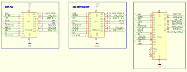
A minimization of the original equation I verified with U87 can be written as follows:
!END_CYC = Q4 # RAS & !RES_0WS # AIOW & !RES_0WS # !IOR & Q1 & !IO_CS_16 # AIOW & Q1 & !IO_CS_16 # RAS & Q1 & FSYS_16 ;
!END_CYC =
Q4
# RAS & !RES_0WS
# AIOW & !RES_0WS
# !IOR & Q1 & !IO_CS_16
# AIOW & Q1 & !IO_CS_16
# RAS & Q1 & FSYS_16 ;
From this AND/OR equation you can see that FSYS_16 taken with RAS=1 and Q1(timing of CPU bus cycle) results in !END_CYC being active low when this term is true.
So this occurs more frequently when only using Q1 and RAS in our state evaluations of this last test, resulting in more 0 reads of the output.
The CPU cycle timer which generates Q1 and Q4 was designed by IBM as a function of the inverse double CPU clock and /ARDY, the signal which controls the READY state for the CPU to exit the command cycle.
The logic level of /ARDY going through the cycle timer is controlled by /END_CYC which resets /ARDY to 0 logic level at certain moments. When /END_CYC goes active low, the cycle timer starts running, otherwise it will remain in RESET.
Eventually the timer will advance at double CPU clock speed to let Q4 give off a positive logic pulse. That's my theory, since this occurrance might be very brief to let a single "1" state of Q1 be able to clock through to Q4. I believe they created this circuit by running tests to see if a pulse could be generated using this release-from-reset method. Q4 will become active after two CPU clock cycles, or 4 double CPU speed cycles. So Q1 and Q4 are logic 0 most of the time, and only provide positive pulses sequentially after being initiated by /END_CYC going active low.
!END_CYC seems to be activated when memory reads or writes or IO writes are occurring, using the terms
# RAS & !RES_0WS
# AIOW & !RES_0WS
And then "synchronised" using terms with Q1 and Q4 which are only then generated after RAS(memory read or write) and AIOW(IO write) activate it while !RES_0WS is inactive high.
That's what I am seeing when looking at these circuits and equations together as a whole.