• Please review our updated Terms and Rules here

Project to create an ATX 80286 mainboard based on the IBM 5170

I can only say: WOW!

Question out of curiosity: why did you use a VGA card and not a CGA or MDA card? When running the VGA-BIOS, you could have run into a bug activated by the software and a POST card would not be helpful here. Possible answer: you don't have such a card and monitor?
 
Hi mogwaay,

Thanks for the encouragements, it's much appreciated and great to see your post here.

I was also surprised that I got some screens working already at this phase since I have made so many changes in one go to reach this design step.
I know I should have done the "inbetween" steps but I was hopeful and optimistic it might not be necessary.

I made a list of possible causes and I am doing a lot of work to check all the things.

I am starting to see something related to the keyboard controller init which appears to occur just before the CPU stops running.
I can see the keyboard lights flash briefly just before that.

It may be a coincidence and of course the self tests will run really fast, it may be only apparent so I need to make some sort of post code display to put on the latch port since I don't have a post card yet. Something to put on my list of things to do. I will update more about what I tried and observed in another post when I get more things done.
 
Hi Ruud,

Thanks for the compliment, I am working hard to narrow down the problem, so far it's not too clear what the cause is yet.

I do have a ATI Small Wonder card and monochrome CRT, I was not sure if it is going to work before so I didn't test much with it yet.
Apparently I need many resets to get enough CPU cycles to initialize the VGA, so it could be possible that this condition of being able to run a number of CPU cycles also can result in initializing the CGA card.

I will have a try and I will update the findings here as soon as I know more.
I did originally start out testing with the CGA card on the first tries of powering on but I was not aware of the init being able to partially happen after more resets so I changed to a few VGA cards. After testing more I found that other VGA cards also do initialize so it's possible the CGA will work after all.

Thanks for the idea and reminder that this still may be an option.
I added this to my list of checks to do and will post here what happened.
 
It appears that - if - the CPU can keep running, which needs a number of power cycles and resets to get a good startup of the CPU, more stuff will happen and get detected etc.

It doesn't appear to be a problem detected by the POST which stops the system from POSTing further persé, but rather the CPU is crashing before it can get around to anything. That is what it is looking like but when I have more findings this may change yet. The CPU stops around the moment when the keyboard controller is initialized. This happens when the BIOS reports the CMOS error and asks for keyboard input to update the settings. Somewhere around that time something appears to happen that stops the CPU from executing further code. Another thing worth noting is that the speaker is not beeping on the error which is what should be happening. The CPU stops running before the beep tone is played on the speaker however.

I am also working on the CPLD programming because the POF2JED program asks for various parameters. I do have a PDF guide which describes the options. It's a little unclear because the guide talks about disabling or enabling, and sometimes the language is vague and not clear on which setting results in enabling and which disables. And I have three CPLDs needed for the system so if I change something I need to convert three times and ISP program three times. I tested ISP since now the CPLDs contain known code and it's safe to do so, and I am able to update while the CPLDs are on the mainboard which does save some time.

One of the options I am updating now is the "slew rate" setting. I started out with "slow" because that was said to be more stable, and now I am updating them with the "fast" setting to see if any change. I only need to update the memory decoder now to the fast slew rate setting.

There is also something strange happening in quartus because it assigns a setting of "open drain" to bidirectional pin XA0, while not doing this at bidireactional pin XBHE, which is strange. I have searched in quartus all over the menu's and items but I can't find any manual configuration of this property of the bidirectional pin.

Possibly quartus is doing this by itself because of the circuit however it is very similar in both cases so I don't see the difference warranting a different setting.
When opening the list of pins I can see it, and also using the "technology viewer" window it reports after the pin that it's open drain. Since I found no way to edit this feature yet, I have added a pull-up resistor to XA0 just to be sure this is covered in case of the pin not being able to go high during DMA. Though possibly the init is not getting far enough yet to check the DMA controllers.

If anyone reads this who can give some comments or descriptions on quartus from their experience about the issues I mentioned I would appreciate to read about this. It appears that quartus automatically assumes the output pin mode to be programmed according to what is connecting to the output in the schematic design, but I can't know for sure yet. I am going on this assumption for now. Later I will check all the source and output files made by quartus from the project to see if I can read any clue about this in there.

I have a few keyboard controllers and I will test all of them on the IBM and ARC board just to rule out some things. Also I am going to check all the pins of the keyboard controller on the IBM to see their default state on good inits and compare with the new design. I also changed the clock input compared to the IBM way however it is based on information I found and previous tests on a Z80 mainboard which worked fine.

I mostly am trying to test with the MR BIOS generic 286 without turbo option because that most closely matches the system. I don't provide any turbo mechanism on this revision and I don't like the method of enabling several port pins on the keyboard controller which MR BIOS may be doing in those versions because this may trigger other things to happen.
 
Last edited:
I have done a lot more testing. I took out more ICs on the 5170 mainboard and soldered in more sockets for testing.

I tested all my keyboard controllers, they all work on the 5170.

Next I proceeded to exchange all the 74ALS573 latches on the 5170 for sockets and tested with 74HCT573, which works completely fine on the 5170 as I expected.
The 74HCT573 is a much more available part than the ALS version.

I will do similar other replacements in the future to see which more common parts are compatible with the 5170 AT, which also should be compatible with my prototype.
I tested all the 82284 and 82288 system support chips I have and I found to my surprise that some of the 82284 were not working with the 5170.
So they must be marginal or incompatible. So I marked those and I will not use them for testing.

I have also come a little further with the prototype debugging. I have not found the cause of the CPU crashes,
however I have found that when I insert the coprocessor, -if- the CPU comes up with a stable databus on power up, the system is now even bootable and controllable by the keyboard.
There is a lot of screen corruption but the PC runs mostly completely stable.

I was able to do Checkit testing and the whole mainboard tests as completely OK.

I did the memory test of Checkit - also completely passes all the tests.

The DMA channels work and also the IRQ functions are correct according to Checkit.

The coprocessor is also fully functional with my own circuits based on descriptions by Intel and IBM in their datasheets and manuals.

I am able to boot from harddisk via XT-IDE option ROM in 8 bit mode (!) and I can boot from floppy drive.
So the 8 and 16 bit selection logic also works 100%.
The option ROM works in 8 bit mode but the IDE interface is of course running in 16 bit AT mode, so not needing any conversion on the IDE connections.

I can format a floppy disk with no problems, so DMA is not only passing all the tests but also passes the most difficult test - to format a floppy disk.

I can run Norton Commander, copy files, read all directories on the harddisk.

I can also SYS a floppy disk to make it bootable and copy over more files to the floppy drive.
Floppy boot itself also works fine.

I can run windows 3.0 and start a patience card game for example.
I need to make a small board for the USB to serial solution so I can use a wireless USB mouse as intended.
There is also a problem with the UART not showing up in the BIOS yet. I will try with a different UART chip in case it's faulty.

I have tested the CPU and NPU with Landmark 6 which runs fine and shows normal performance corresponding with the clock speed.

I have run the game Wolfenstein 3D which also runs the demo without problems.
If there is any memory problem in a system, it will definitely crash this game as I have seen happen.

So from all these things I can conclude that the 8 to 16 bit data conversion works 100%, the SRAM memory decoding system works 100% fine.
The CPU runs stable with the coprocessor added to the system.
It's possible that the coprocessor is stabilizing the data bus on the CPU side, or possibly there is some kind of test running by the BIOS which depends on the coprocessor being present.
Or maybe something is triggered by the NPU logic in the CPLD which then needs the NPU to be present in the system.

At the same time it is also possible that there are other issues which I have not discovered yet, but it is narrowing down and shortening the list since I have been able to test many more things today.

I am still doing tests and working hard to find out what is causing the power on to not have the CPU running stable on many occasions.
What happens is I need to turn the PC off and on a number of times until the CPU comes up stable.
After that it keeps running properly. It is reset and CTRL-ALT-DEL proof and comes back up.
Only a power down will make it necessary to try a number of times until a next stable power up occurs.

Strangely enough I also observed this problem with the first ARC mainboard. So it is quite possible that one of the transceivers or latches which I took from that PCB is marginal and is causing the problem.
So I will be desoldering all these chips on the prototype and replacing them with others.
Many chips don't need to be ALS types persé so in that case I have more new or working used parts available in my parts supply to start replacing more ICs on the prototype.

There are also a few more remarkable things which I am looking into:
- the voltage on the S-databus is raised by 1,65V after powering on the system. This 1.65V is somewhere in the middle of the databus waveforms when they become active.
Kind of like a 0V line of a AC signal and the AC wave is going above and below that line, that is what I am seeing on the scope when the CPU comes up.
- I don't know if anyone has looked into this before, but if I measure the substrate "CAP" pin on the 286 CPU, it charges the capacitor to -3.7V.

I have done some capacitance measurements on a bare PCB and I am getting 2.20pF and 3.32pF on pins 7 and 8 of the 82284, and I am getting 33pF on the 286_CLK output line which goes to the system controller CPLD, the CPU and coprocessor. So I may lower the load capacitance on the inputs to have a try if that gives any improvement on the wave shapes. I think the 286_CLK signal is not looking very great but I have seen similar clock signal waves before, it does not persé pose any problem. If the clock is unstable usually it will result in divide by 0 errors and being thrown out of windows. I didn't see such things happening so I believe the clock pulse is not likely to be a problem, though I also don't exclude that. I am still looking for a method to improve the clock wave shapes on which I have done some research. Possibly it is better to input from an oscillator into the external frequency input of the 82284.

So, I am not there yet but a lot of things are working properly. All the test software is not finding any faults at all.

We now have:
- fully working 16 bit SRAM memory subsystem (15MB capable) functioning as designed on the ISA slot
- BIOS ROMs working in 16 bit mode
- option ROM 32kb in 8 bit mode, the user can add any ROM images together up to 32kb, which will be mapped to 0C8000-0CFFFF region.
- UMB blocks of 128KB between 0D0000 and 0EFFFF to load DOS and TSR device drivers etc high
- system runs stable for hours after getting a functional power up by doing a number of power cycles
- the keyboard controller functions 100%
- the RTC is working well
- DMA controllers work
- Interrupt controllers work
- the system timer works
- the LPT port is detected so it should work
- ISA slots appear to work fine, I will do some tests with a sound card
- all 3 CPLDs appear to function as intended in the designs

What still needs to be done is:
- the UART didn't show up so I need to check this further, may be a faulty chip
- get a stable power-on every time
- fix the screen corruption problems
- test with XMS memory populated on the memory card, all footprints are fully decoded
- solder the ethernet chip and EEPROM to the PCB so I can test 16 bit LAN functions
- find some 53C400 chips so I can test SCSI but there is no reason it won't work from what I have seen in the tests so far

So many good news for everyone interested in the project and thread!
I am not there completely, but happy for all the things going right.
The most difficult hurdles and design changes are taken and verified, now only to get the final problems out of the system!

I will upload a few photos and screenshots.
So cool to see the 8 bit conversion LED lighting up when formatting a floppy disk for example.
This really shows the complexity of the AT system more when you watch that LED!

Kind regards,

Rodney
 
Last edited:
Some photos and screenshots to share the happy news

And I forgot to mention, the onboard primary IDE interface and floppy drive interface are also fully functional.
The secondary IDE I still need to test, I need to create a new XT-IDE AT version ROM which includes the secondary interface.
Then it should show 4 drive detection lines in the option ROM message text.
Also, IDE CD-ROM drives should work fine which I will test.
I will also do some testing with a soundcard using wolf3d and also play some music in modmaster.

More news will follow as soon as I have it.
 

Attachments

  • Img_3591s.jpg
    Img_3591s.jpg
    155.3 KB · Views: 11
  • Img_3584s.jpg
    Img_3584s.jpg
    138.4 KB · Views: 9
  • Img_3578s.jpg
    Img_3578s.jpg
    125.9 KB · Views: 10
  • Img_3576s.jpg
    Img_3576s.jpg
    1.1 MB · Views: 10
  • Img_3570s.jpg
    Img_3570s.jpg
    169.2 KB · Views: 10
  • Img_3546s.jpg
    Img_3546s.jpg
    38.9 KB · Views: 11
  • Img_3568s.jpg
    Img_3568s.jpg
    150.9 KB · Views: 11
  • Img_3542s.jpg
    Img_3542s.jpg
    203.8 KB · Views: 16
  • Img_3534s.jpg
    Img_3534s.jpg
    322.6 KB · Views: 17
  • Img_3527s.jpg
    Img_3527s.jpg
    208.1 KB · Views: 15
Last edited:
I have browsed the whole thread but have not found an answer. Does reading PAL chips with an EPROM reader require soldering the chip off the board? Can this be done with the chip in the board?
 
Hi rask,

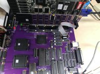
Yes, it would require desoldering the PAL chip from the board.

Desoldering anything from a PCB, and even working with it and handling it, connecting, disconnecting etc. all carries risks. This is always the own and sole responsibility of any person who uses the information in this thread and anyone working on a board has to - before hand - start by accepting all the risks it carries.

Desoldering a part is a risky venture. Anyone who does this needs to accept that they have a big chance of damaging the PCB. Double sided PCBs are sensitive to damage because they have through metal plating which needs more care to remove the solder from all the holes. The holes connecting to VCC or GND are more difficult to desolder because they need more time to properly be able to liquify the solder throughout the hole and to the other side of the component. So enough heat and duration is needed in the first place. Next is to have enough suction applied to the liquid solder and sucking out as much solder as possible. After removing all the solder as much as possible, I found that the best method is to use hot air to once again liquify all the solder throughout all the pins of the IC. By holding the IC with a IC puller and clamping the PCB while heating the bottom component area, there will be a certain moment when you can feel with the most gentle movement possible that the component is completely "loose" in the PCB and that is the right time to extract it from the PCB.

Another few pointers: many PCBs have the IC pins bent at the factory to fix them onto the PCB. An annoying method indeed. So it's best to first use a suitable tool and soldering iron to straighten all the IC pins before doing any desoldering. After straightening it's often a good idea to add a little fresh solder to each pin in order to make better contact and heat transfer throughout the hole and component with the desoldering iron later.

When desoldering it's important not to apply any pressure onto the PCB with the desoldering iron tip because this scrapes and damages the PCB. Using more force will also result in scratches in the solder mask if the desoldering tip comes away from the pin, and it could bend the wrong way which you don't want. So it's important to be careful. Using good stong light and magnification allows you to better control your actions, especially for those of us above 50. ;)

Also it could be beneficial to preheat the component area from the bottom side before starting to desolder the pins. So heat before and after desoldering while extracting can be very useful. Care must be taken not to melt any plastic parts. This even happened to me with the connector on the memory card which melted due to the heat. I use a paint stripper gun right now because this is more durable than the cheap hot air tools and it was easy for me to buy. The one I bought has two settings and I use the lower power one. Next it's a matter of controlling the distance to keep far away enough to get exactly the right temperature of the component area and not overheating because of the strong power of that tool. I need to make some kind of nozzle to focus the hot air, which could improve the tool more. Right now I have gotten to a skill level and experience with that tool that the PCB is completely fine after using it. I practiced a lot with some old PCBs.

Theoretically one could try solder wick to remove most of the solder and then apply hot air to the whole component area before extracting it. The wick does carry more risk though to pull off traces or pieces of the pads when the solder becomes solid before removing the wick strip.

Again, anything a person does with the information in this thread is at their own sole risk!
I want to help anyone I can but in the end you are yourself responsible and always taking a risk when doing anything with a PCB.
Before hand one has to accept that the outcome will be a damaged and broken PCB.
I bought and used a total of 4 mainboards in getting to the stage I am right now. Two were very marginal and the other two have been heavily soldered on.
Thankfully I was able to keep them running. One of the working boards even needed a lot of repair because of battery chemical damage to all the traces. After desoldering a quarter of the PCB and cleaning it, neutralizing the chemicals with vinegar, I was left with broken traces because they were already almost eaten through by the chemical damage. And thus I "broke" the PCB and needed to beep out and fix several traces. Everything you do has consequences which you need to accept or else don't start it at the first place.

Even asking a professional to do some desoldering work for you still carries some risk because there is no perfect situation. Any professional person will warn about this risk. Old PCBs and components can be vulnerable and marginal already and working on them can give them more defects. And equipment of that age around the 90s is now around 30 years old which also tests durability of parts. As I also commented before, possibly PAL components can go bad with ageing, so reverse engineering work is extremely important so the technology doesn't get lost, especially with historically meaningful electronics.

Kind regards,

Rodney
 
I have done more testing and I have found one of the factors in the problem where I need many power cycles to get the CPU to stay active.
I now have a correct power cycle happening after powering off and on about two or three times which is a huge improvement, previously I needed more than 20 power cycles.

I originally started out with the concept to clock the DMA controllers at 4.77 Mhz to get more performance, however apparently this seems to be causing some problems.
I found this out by changing the DMA clock to 4Mhz. After I programmed the update I immediately noticed a change where the CPU is much more likely to have a functional power-on state when the DMA controllers run at 4Mhz. I will keep testing with this new DMA clock frequency from now on.

I also did many tests with the bus transceivers. I exchanged all the transceivers and latches with sockets and tested with exchanging the ICs while holding the system in reset and keeping it powered on.
After the new part is in its socket I released the reset jumper for testing.
The only exchange which was a little risky was the high to low byte conversion transceiver. After that the PC didn't come up anymore. It was a little difficult to get to this IC because it's between the ISA slots. So I exchanged all the parts to originals and after a number of power cycles I got the system up again.
Anyway, no exchange of any transceivers appeared to improve the situation with the screen character corruptions.
What I am observing is that the screen characters are not updated in the whole screen, but rather the screen memory is keeping the previous values instead in various random positions.
When scrolling the text screen down it appears to scroll away the incorrect characters upward until they disappear at the top edge of the screen.
This is one way to get the screen to reasonably clear itself of incorrect characters. So the problem appears to show itself when updating the screen character memory.

I also had a good look at the clock pulse generation by the 82284. I exchanged the load capacitors of the crystal with two sockets so I could test out many values of the capacitors.
I discovered that the capacitors are not too narrow in their requirement. In many combinations the clock output is working, however there is some difference in the phase symmetry. So this I believe explains the difference in value between the two capacitors from the datasheet. In fact, even without load capacitors the 82284 starts oscillation just fine, I expect it's the PCB capacitance of a few pF already is able to function as a load capacitance by itself. I will keep experimenting and set some reasonable values for the two capacitors. When the power on cycles were worse than they are now, I found no improvement by any variation of capacitance in the load capacitors. I could try some trim capacitors to see if I can determine the best clock symmetry possible and then measure the set values to know the ideal capacitances. Unfortunately my cheap scope cannot be trusted to precisely measure the clock frequencies so I am not sure if they are completely stable. When I "zoom" out, this scope seems to be better able to count the number of cycles and calculate the cycle frequency.

After changing the DMA clock frequency I am seeing more improvements besides the fact that the system is more likely to power on in functional state.
I also saw that Modmaster is now working to play songs when previously it was not able to.

I will also exchange the UART chip later because it may be defective. Possibly there is some other issue with this chip so after removal I will test with a serial port card to see if the MR BIOS can detect that.
 
Apparently the problem of needing many power cycles is not gone yet. There was some fluke which caused a few sooner stable cycles but later the problem returned and was the same.
Also when test exchanging the load capacitors on the 82284 clock generator which occasionally caused the clock to stop and start running again I once experienced that the CPU suddenly came up stable and ran after a clock interruption without needing any power cycle.

Another thing about those repeated power cycles being needed, after every power cycle the data bus behaves differently and is showing different wave shapes. Sometimes they are "quiet", sometimes some strange shapes, sometimes repeated patterns, and when the databus bit is showing patterns looking like normal activity of a computer, these patterns are also varied. When the system is actually running, I am seeing two different amplitudes alternating eachother. One is around 5 Volt full amplitude, the other is maybe 1 Volt lower.

I have done more testing, I exchanged the MC146818 with a DS12885 and changed the jumpers. After that the DS12885 is also working properly and can be used as a RTC and CMOS chip.

I removed the UART chip and left it out for the time being. I will test the system first with a serial adapter card I have. Then I will see further how to get the UART to function. The chip may be defective so I will test it on that adapter card as well. However also no change to the power cycle problem after removing the UART chip.

I added two more SRAM chips to the memory card so now there is 2MB of SRAM on the card.
After getting the computer to power on stable, the MR BIOS correctly detects the new memory and registers it as XMS memory.
Also, the 64kb high memory area becomes available after loading HIMEM.SYS.
DOS is now high loadable as well and reported as loaded to the HMA.

I tested the game Wolf3D and it is also correctly seeing the XMS memory.
So it looks like the memory card should be fully functional in being able to provide the 15MB total of XMS.
Of course, I didn't test that full amount yet, which would need 30 chips, but since the XMS is properly decoded and detected, and can be used by DOS and for games, I can assume that the rest of the memory space will be functional as well as soon as the chips are populated. Later I will solder more chips to the board so I can try to use the memory.
 

Attachments

  • Img_3616s.jpg
    Img_3616s.jpg
    184.1 KB · Views: 6
  • Img_3617s.jpg
    Img_3617s.jpg
    220.8 KB · Views: 4
Last edited:
Rodney, your work is awesome!
Your board looks beautiful!
You have put a lot of work to it, and a lot of knowledge also.

Would it be useful if you change temporally the clock circuitry, so that you can select between full speed and a very slow clock, even a step by step clock?
Also, perhaps it could be useful, to create an add hoc tool, so that you can trace the CPU instructions being executed. Although that would be a very raw listing, that would have to be disassembled, and, even then, very difficult to read.
Perhaps it is possible to identify points in the execution ot the ROM startup, specially if the ROM you are using is a open-source one.
Perhaps it could be useful to compare the CPU instructions being executed (step by step), comparing them with the signals, for example at the ISA bus, using a logic analyzer.
Is also possible that the board works stable at very low speeds, and that would suggest a problem with timings or a "bad shape" of an electric wave signal (I also talk on it below on this e-mail).
May be, it is possible to design a device that goes single-step (or at different slow clocks) and debug the execution to the point where it fails. I have seen one for the Z80 processor.

From my so little knowledge, perhaps your problems could be caused from an unstable or bad shape of the electric wave of some signal, that leads sometimes to the circuitry at some point to take a wrong binary 0 or binary 1, and messes with the whole board?
Regarding this point, perhaps it can be useful for you the experience of S M Baker building a PC XT computer with Sergey Kiselev design. For the most part, It worked for him ok. But he found sometimes a unstable functioning (I don't remember the details), and S. M. Baker posted a video that include his investigations trying to solve the, under whatever circumstances, a sometimes rather unstable functioning. I have to search for that video.
Although I have to make a spoiler: S.M.Baker did not solve those problems completely, although his investigation could be useful for you, given that S.M. Baker is a so experienced guy.
If you want, I can search for that video and post it here.

Also I suspect your problems are only caused by a defective chip. although you have tested and traced many of them , if not all, for my understanding.

I have still to go through all of the postings on this thread, and correct me if I am wrong, but I think your design has some PALs and/or CPLDs. Would it be possible in the future to substitute them with discrete logic, with individual TTL chips?
Perhaps impossible? Or perhaps would lead to a excessively big board?
Perhaps it is not necessary, if we have the complete source code which with all of those PAL and CPLD have been programmed. You have all the source code?

Last, I will like to ask you if, when your 286 board works completely. Do you plan to make afterwards a second version, that based on the 286 desgn, and using "rehsd" interface between 286 and 386sx, could lead to a complete and functioning 386sx computer? In that case, it would have the advantage of being a computer with protected mode for a multitasking operating system.

I hope I have not repeated previous questions or already answered points. If yes, sorry for that.

Regards,
Alvaro Garcia
 
I correct a previous errata I wrote:
"Also I suspect your problems **could be** caused by a defective chip. although you have tested and traced many of them , if not all, for my understanding."
 
Hi Alvaro,

It is great to hear from you! And thanks for your compliments, I appreciate that.

Getting to this first prototype is a very important milestone for me to recreate the amazing AT design.
I have a lot of appreciation and respect for the IBM AT designs and concept by Don Estridge.
After studying all the circuits in much detail the work I have done and I am continuing to do is revealing more and more of the intricate mechanisms involved in the functioning of the AT PC.
And of course to understand the Intel 80286 CPU in deeper detail. It is much more complex than a Z80 for example.

What you suggest certainly would be interesting to explore, I mean I know the idea of stepping through the instructions like done in the Multitech Micro-Professor MPF-1 for example.
We used this little computer somewhat in school and I fell in love with the beautiful circuit board with those calculator style buttons and the 6 beautiful LED display segments.
In fact, I have copied the schematics in my schooldays when I was an intern doing the IT management of the school, meaning to build one.
And I have done so, a few years ago I built my own version of it. I won't publish the designs because these things are still being sold as commercial product.
I built one using cherry keyboard keys. At the time I didn't follow through to do more with this computer. Multitech (Acer computers) made a few revisions of computers with increased sophistication.

If the 80286 can be "slowed down" without crashing the CPU I am not sure. In this case since the computer uses SRAM maybe it is possible to do so since refresh is not needed in the CPU's SRAM at least.
Of course we could replace the crystals with slower frequencies and see what happens.
However there are a few problems for using this approach:
- there are too many lines of code involved with the BIOS
- there is no "open source" version listing of the BIOS
- I am just too inexperienced at the moment in assembly programming on the 80286, not even a novice.

There are so many aspects involved in PC technology that it would take a long time to fully master everything. Though of course it is extremely inviting to dive into this technology.
We see traces of everything in diagnostics software, we have hardware interrupts, software interrupts.
We have protected mode which is also present in the 80286.
The XT concept "lives" within the AT concept in order to provide backward compatibility with 8 bit PC technology.
We can plug any 8 bit card into the AT and it should run.
When I start my AT prototype, I have provided a LED to signal when the AT is doing 8 bit execution and data conversion.
Which is so interesting to observe, when the AT is running 8 bit code, or accessing 8 bit hardware, you can see the changes in the bit patterns of the higher data bytes which is also telling to show that the AT is converting the codes and byte access.

I started out this project with the concept of doing a "pure TTL chip" design. However as commented here in this thread, this would require too many components as has become apparent. Inside the PALs and PROMs is a lot of logic and decoding which would require a large surface to do this in TTL. Which is certainly one of the reasons why IBM did the design in that format in the first place. It is too impractical to do the pure TTL approach and I abandoned it. Besides all the considerations there is also the consideration of the large volume of ICs needed which would have to be sourced and bought. For me there is no way I am going to go in that direction especially since I am now using CPLD technology which is already a step further in development capability. Using CPLDs greatly reduces the PCB area and numbers of ICs needed, and provides a proper flexibility needed for this project scope. Basically the format of this project is the best approach I can come up with so far which is practical to achieve. After the project is finished I can consider alternatives such as FPGA and CPU emulation etc.

Playing the Wolf3D demo on the screen is a great way to show the 8 to 16 bit conversion where you can see the flashing patterns of the conversion LED, which is why I provided this LED.

I will not be doing any 386 projects, the 80486 is a possible consideration for a future project, however this also depends on how I will feel looking back on this project in the future.
And I want to play around with 486 mainboards and technology first to see if and what is possible in this regard.
This project has been and continues to be a huge task to complete and I will need to reflect back on this in the future if I want to explore further development along the path of PC technology.

Producing this prototype was not cheap, the whole project was very costly for me, much more than I envisioned initially.
I will only build another revision if this would really be of great value to the project.
I may or may not just design a revision but not build it, if the concept is already sufficiently proven in this revision anyway.

First order of actions is that I need to determine where the observed problems are coming from. This is the first focus of my work now.
If any PC experts could provide thoughts, ideas or clues feel free to comment anything especially if the information I provided leads you to have some idea about the causes.
In fact, it doesn't matter if the comment is valid or not, it could at the least inspire more ideas to be exchanged.

There are a few things which stood out to me so far while doing the debugging and testing:

1. the big variations in data bit patterns which are shown each time when I power cycle the computer literally shows different patterns on each power cycle. What is more strange, the CPU after starting to actually execute, does keep the stability for the most part no matter if you reset it 100 times or leave it running for a whole day. It just keeps running properly unless it is crashed by my actions on the hardware side or I power cycle it again.
It's like this: I need to power cycle the computer maybe 30 or 40 times, and then suddenly it powers up properly. The beeper speaker then sounds a BIOS beep which is the right tone frequency, but the duration is much too long, but not always(!). Sometimes it is the proper length, but rare to occur. Mostly it's too long the duration. Same with the MR BIOS "delay" counter when cold booting the PC. Sometimes the seconds counting down the user defined delay time from the CMOS settings are normal, but most of the time they are much slower than they should be. Like twice or three times slower counting the seconds. Though the stability is always just fine.

Another "symptom" is that certain software won't run stably but this may be a display corruption reason that I am not seeing what the program shows and this led me to believe a crash occurred. For example the MS-DOS program EDIT.COM/QBASIC.EXE I can't bring it up properly so I used Norton Commander for editing CONFIG.SYS. Also disk copy fast doesn't seem to run properly. As I commented, the floppy drive works perfectly through the onboard controller and is not the problem. Also 16 bit IDE is working fine. I will make a XT-IDE ROM file to support both the primary and secondary IDE interfaces for testing soon as well.

The UART was having some problems which I will explore. Everything will take time to fully test all the system functional aspects. Each time I am testing more things.

2. a strange DC "offset" in the data bus transceivers, which is sometimes even a full 100% DC level resembling a constant full "1" value on the bit, before the CPU starts to execute, that is, if during that power cycle the system does anything resembling execution of code. Of course, it's not a true offset but rather could be called a start logic level before execution of data code begins.

I have done some testing by Checkit 3 and it cannot identify any malfunctions. Maybe there is a problem in the system timer I am not sure.
I am using the system controller CPLD to provide the TCLK timer clock pulse from the OSC input. This is first divided by 3 and then by 4 to get down to the 1.19Mhz.
I saw the symmetry is slightly off. My scope is not too great to show this properly.

There is also another thing I am considering to test out, and I will. The CPLDs have a power-on reset function which can be enabled when programming them. I still need to try this to see if that could give any improvement in stability. Possibly the state of the CPLDs at power on is creating the problems. There is also a "pin keeper" option to keep the inputs at their last levels but this seems to be related to standby power down functions of the CPLD which I am disabling.

And there is another matter I remember, while testing the 4 286 mainboards I have, sometimes I experienced similar problems where I needed multiple resets or power cycles to get an accurate functioning happening. Notably with the first ARC mainboard I experienced this. And while doing some testing with the 5170, at times I also have needed a few power cycles to get it to POST.

What I need is a decoder to translate the POST output bytes into readable form using two LED displays. I already have included a latch which provides the latched bits and connector for this purpose to wire this translation display, I only need to make the translation part which also will cost me some time to do. Seeing the POST progress before the CPU crashes may possibly be useful to provide further clues where the error is caused. Anyway, as I commented before, sometimes the CPU is in such a inoperable state during a power cycle that the data bit pattern looks totally weird. That pattern is indeed observed more often during non-functional power cycles.

I am continuing to work on solving the problems observed, it takes time to do all this work. I am compiling a list of debugging notes from theories and findings and working to explore and eliminate things on the list.
 
Last edited:
Ok, whatever path you take to continue debug the problem, it would be a good path.
It is a very complex project and you have accomplished already great achievements with this project.
Take it easy , as it implies a big effort to push this forward.

Good luck!
Alvaro
 
A few more things resulting from my work so far.

Possibly the DMA clock frequency was no issue and probably when the power cycle problem is resolved I will return the DMA controllers to the previous 4,77 Mhz operation or even the specified 5Mhz for performance reasons. If I can get DMA to work 25% faster that will be a bonus. Also I will of course experiment with higher clock frequencies for the CPU later. But first I need a stable system of course.

I temporarily resolved the freezing CPU during or around keyboard init in the POST by adding the coprocessor which suddenly removed the problem entirely where the CPU froze after an initial start. I will explore later to see the possible reasons. The fact that the AT does have this problem may or may not be related to the proper CPU operation needing a number of power cycles first. Maybe some fluke in the coprocessor is getting the system to run in the first place. Without the coprocessor I only get the first BIOS events happening to show the CPU type, frequency and detected RAM capacity. Normally it will report the CMOS error with a beep and ask for a keypress which freezes the CPU without the coprocessor present.

I will try enabling the power-on reset option in POF 2 JED first in all CPLDs.

Also I exchanged the system controller CPLD with a different chip, I have 4 CPLDs which are apparently functional out of 10 chips, so I have then taken the previous system controller and replaced it in the IO decoder socket to rule out some defects in the CPLDs but this produced no difference in any computer functions so I don't believe it's an issue.
 
Last edited:
Two more possible ideas:
- burn a ROM chip with software written to debug the initials steps to reset the computer and test it, based on an open source BIOS, and start your board with it
- use a POST card to see if it reports any error
 
I have seen this at: https://github.com/b-dmitry1/BIOS

x86 embedded BIOS R3

Very compact (less than 8KB of ROM space) x86 BIOS for embedded systems, FPGA, and emulators.

Tested with a hardware:

Original Intel 8086 CPU
Harris 80286 CPU <==== !!
Intel 80386SX25 CPU
Intel KU80386EX25 CPU
Cyrix Cx486SLC-V25 CPU
Texas Instruments TI486SXLC2-G50 CPU

Some board images could be found in the pictures directory.

Tested with an emulators:

Bochs 2.6.11 (require USE_ADDON_ROMS and USE_IDE_HDD in "config.inc" to use Bochs's Video BIOS and HDD)
 
Joining the brigade of people with random suggestions: how are you loading the power supply? I know some power supplies get fidgety if you don't load all the rails, or only have a minimal amount of load. If you toss an old hard disc you don't care about on the PSU, does it impact anything?

When it doesn't come up right, does the reset button ever help? I sort of wondered if it was starting before the power supply really stabilized, and ended up in a state where it couldn't recover.
 
I will add one more hypothesis. If, as I think, your board now does not use DRAM and does not have hardware to refresh DRAM:
Would it be possible that, if you are using a "standard" BIOS, that, when it tries to initialize the DRAM refreshing hardware, it could perhaps make the booting unstable?

So I see two advantages to try to use an open source BIOS:
- it would make your project completely open source both on the hardware and the software side
- it can potentially help you debug problems with booting and initializing hardware

The drawback is that is more work, not to say that it is not clear if it is even possible to find or write a BIOS for the 286.
Perhaps I could even try to help on this item, although for sure there are over there people with more knowledge

P.D: even in the case that the previous "dmitry" BIOS is barely valid for your board, it seems that it lacks functionality. But if it manages to domething similar to a boot process, could be the starting point to write a more complete BIOS.
Also take into account, that there could be perhaps other candidate BIOS. Perhaps coreboot or libreboot?
 
Joining the brigade of people with random suggestions: how are you loading the power supply? I know some power supplies get fidgety if you don't load all the rails, or only have a minimal amount of load. If you toss an old hard disc you don't care about on the PSU, does it impact anything?

When it doesn't come up right, does the reset button ever help? I sort of wondered if it was starting before the power supply really stabilized, and ended up in a state where it couldn't recover.
If there is really a chance that your power supply is making trouble, I‘m willing to sponsor one of these neat picoatx supplies - just let me know.
 
Back
Top