• Please review our updated Terms and Rules here

Rainbow 100A Memory beyond 256K?

alitel

Member
Joined
May 9, 2023
Messages
23
Hi folks -- dumb question du jour: Does anyone know if it's ENTIRELY impossible to expand the memory on a Rainbow 100A past the 256k mark? I did acquire a 100B expansion board, but the naive approach of inserting it (it's configured correctly) just hangs the machine immediately. I had seen (somewhere, lost to the internet) a person who indicated a 100A with "maxed" 832k of ram... which gave me hope.

Thoughts, info, views welcome! I am on the hunt for a 100B or 100+ but I do love the 100A with the roaring fans :)
 
For the 100A you cannot use the 100B memory expansion card directly. You need the 8087 daughter card. You remove the CPU from the main board, plug it into the 8087 daughter card, plug the daughter card into the 100B extension board, attach the cable from the daughter card to the CPU socket on the main board, mount the 100B memory card to the main board.

You have to have the 100B memory board loaded with 256K chips to get the full memory amount. I found the 256K chips are readily available online. Note: even though the adapter daughter card is labeled 8087 there is no 8087 on it. Google Rainbow 100a 8087 and you will find information on it.
Mention and images here:
 
Last edited:
Thank you so much! This is exactly the information I needed. that was the post that made me think there was a chance for the 100A, but I misunderstood the nature of the 8087 board entirely. Now, to find one.... :)

Cheers and thank you! A
 
Hi folks -- dumb question du jour: Does anyone know if it's ENTIRELY impossible to expand the memory on a Rainbow 100A past the 256k mark? I did acquire a 100B expansion board, but the naive approach of inserting it (it's configured correctly) just hangs the machine immediately. I had seen (somewhere, lost to the internet) a person who indicated a 100A with "maxed" 832k of ram... which gave me hope.

Thoughts, info, views welcome! I am on the hunt for a 100B or 100+ but I do love the 100A with the roaring fans :)
Yes you can get more that 256K of memory to work on the RAINBOW 100A, but it will require a flew jumper cables. With the 100B memory expansion board you must cut a lead and rewire a couple of connection in order to get it to work.
The Rainbow 100B computers have a extra signal that that they use to detect a 100A or 100B memory card. If the Rainbow 100B detects a b series card it changes some of the memory expansions bus signal lines.
To do a 500K memory card for the 100A is quite simple to get it to work, as it is only one additional lead that has to be wired. For memory above that you must reconnect address line A19 back to its pin on the Memory expansion connector.
On the RB100A memory signals A16, A17, A18 is Not connected.
 
Hi there -- hey, that's brilliant news! I'm happy to do some reworking on the card and/or board -- I could try the simpler 500k mod first and go from there. Would you be ok to share the specifics of the lead that has to be wired for the simpler expansion? (And/or is there a schematic or procedure floating out there that I might reference?)

Cheers! A
 
That's' cool I will have to dig the data back out on how to do it. that might take a while,
A manual for this message that has the memory expansion connector pinout on pages 3-75 to 3-75 is the part number EK-RB100-TM_001_Rainbow_Technical_Manual_Addendum_for_PC100-A_PC100-B_and_Rainbow_100+_Dec84
The website Bitsavers.org computer directory does have Dec and the rainbow 100 under it plus the schematics for the model B . Some of the manuals are also available at Archive.org website.
This manual covers the basics for both models, but there is still some data that it does not cover.
The schematics for the Rainbow 100A and the 100+ plus as far as I know are still not available online, and the 100B have some additional logic chips added and a couple of other changes to its design in general.
 
Thank you for this! I've got a copy of the technical manual addendum and will work away on wrapping my head around the memory expansion function. At a first read, I see what you mean that the 100B switches the meaning of 3 pins on the connector (as well as the NONSHRCYC pin difference) to use them as address bits 16, 17 and 18, rather than (I assume as the 100A uses them) to address 64k blocks 1, 2 and 3 on the expansion card.

Is A19 on the 100B used (regardless of whether the card installed?) to allow for the 128k of onboard memory? (I was a little confused by this).

So, on the 100A, is the general idea of the mod to prevent pin 29 (memory option present) from asserting high (by cutting a trace?) to "fool" the 100A into thinking its a 100A card?

As an aside, THANK YOU for engaging in this discussion -- my hope here is to document this, if we can, for future reference by whomever is interested. Also, no urgency (hobby! :))

Cheers! A
 
Yes you want the rainbow 100A and 100+ to thing it still has a A type memory expansion card.
A19 is used on the 100B for memory operations above the 512K range. The semiconductor device number that I listed are on the RB100A_component Location sheet that I attached to this message.
..
Most of the signal you need are located on pins of semiconductor (ic) device E104. But for a buffered A19 signal - this model has some unused gates on a 4050 CMOS device chip that will work.
This chip is numbered E8 that will take some trace reworking to accomplish it. Some trace cuttings and a couple of lone lead runs to do this. (due to its mother board location)
Some 3Rd parity memory boards don't need it buffered so it is just a maker of running the new jumper lead right to the A19 Address pin on the Memory Expansion Card.
In order to use a 100B memory card in a model a or plus version it is important to hard wire the IO//M signal available at semiconductor device E104 directly to the correct pin on the memory expansion cards.
This is pin 30 on the 100B memory expansion cards. The other old model 100A, 100+ traces related to those pins should be cut (mostly just before the memory expansion connector, as there are being mostly
replaced at the edge of the Memory expansion Connector bus connector with the new ones that run to different signal locations.
The pin number 12 on E104 should be cut off at the base of the circuit board and pin 11 connect to the base of pin 12 on the circuit board so the inverted Address line A18 is reconnected to the memory
expansion connector through the existing circuit trace.
..
I have attached the component layout for the 100, 100+, 100A model and the schematic page that has the low order memory decoder chip.
I have also attached our own sheet about the differences in the memory decoders, these should help speed up your progress.
..
 

Attachments

  • rb100A_Component Location.pdf
    112.6 KB · Views: 6
  • rb100-schmatic-pg1 of 13.png
    rb100-schmatic-pg1 of 13.png
    634.5 KB · Views: 9
  • ram_expansion100b.pdf
    2.1 MB · Views: 6
  • RB100B_MESlot _schematics (cleanedup)..png
    RB100B_MESlot _schematics (cleanedup)..png
    93.3 KB · Views: 9
Thank you! This is fabulous! I would like to try to enable the 512k option first, as being simpler from a rework point of view. If I can get that working, I'll work on reconnecting A19.

My understanding of the procedure for the 512k mod so far is (please correct me if I've misunderstood):

a) Connect pin 5 of E104 (IO/M) to pin 30 of the memory expansion connector and cut any existing other traces to pin 30, allowing straight IO/M signals into the 100B memory expansion card (which it is expecting)
b) Connect pin 43 of the memory expansion connector to E104 pin 11 rather than E104 pin 12 so that we get inverted A18 (we already get inverted A16, A17)

I had a couple of questions first:

1) Does pin 29 (Memory Option Present) need any rework? It seems to me to be used to control the operation of a 100B mainboard and is not used by the memory expansion card itself? So perhaps not?
2) We are sending inverted A16, A17 and A18 signals to the 100B expansion card, but is it not expecting normal (active high) memory addressing? Does this not cause a problem? Or do we just end up "scrambling" the RAM layout but it works anyway?

Best, A
 
Hi there -- I found time today to try out the initial mods to get the 100A to 512k. Sadly, I've not been able to get it working yet. I've re-routed the IO/M signal to header pin 30 (I have continuity back to the 8088) and connected pin 11 on E104 to header pin 43, removing the connection to pin 12. The trace to header pin 30 is on an inner plane so I had to hunt for vias -- I found one trace route (which is where I connected the IO/M signal) and cut the trace outboard of my new connection, but perhaps there are other parts of the circuit I haven't disconnected yet.

In any case, I simply get a hung system on powerup. I've tried grounding connector pin 29 on the 100B card (no change) and tried various combinations of the dip switch settings on the 100B card (also no difference). I will hunt down the LED codes when I get a chance (I either get leds 1-3 solid on, or all leds solid on). I was unable to find any connections to pin 29 on either my 100B card or on na103's schematics for their revised 100B adapter. So perhaps I've missed something there. (My 100B card is a stock DEC one, currently fully populated with 3 banks of 256k)

The 100B card is tested good in a 100B rainbow that I have. The 100A rainbow works fine with and without a 100A expansion card. Perhaps my machine is of a revision that doesn't work with this mod, or perhaps there's a ROM version issue (I thought mine had the latest but I'm not 100% sure). Perhaps A19 needs to be connected differently for it to work? Or perhaps there are additional firmware steps needed. Or perhaps I've just messed something up lol, which is entirely possible. I will review my changes when I get a chance, not able to work on it for a short while.

Any thoughts welcome!

Cheers, A
 
Thank you! This is fabulous! I would like to try to enable the 512k option first, as being simpler from a rework point of view. If I can get that working, I'll work on reconnecting A19.

My understanding of the procedure for the 512k mod so far is (please correct me if I've misunderstood):

a) Connect pin 5 of E104 (IO/M) to pin 30 of the memory expansion connector and cut any existing other traces to pin 30, allowing straight IO/M signals into the 100B memory expansion card (which it is expecting)
b) Connect pin 43 of the memory expansion connector to E104 pin 11 rather than E104 pin 12 so that we get inverted A18 (we already get inverted A16, A17)

I had a couple of questions first:

1) Does pin 29 (Memory Option Present) need any rework? It seems to me to be used to control the operation of a 100B mainboard and is not used by the memory expansion card itself? So perhaps not?
2) We are sending inverted A16, A17 and A18 signals to the 100B expansion card, but is it not expecting normal (active high) memory addressing? Does this not cause a problem? Or do we just ?

Best, A
1) Yes the memory present signal must be at the the logic level the the 100+, and 100A want and not the 100B level. It is normally Grounded on the 100A
2) Really depends on the Memory cards origination of the memory blocks,. Some cards use a different address bus origination so the memory address per Memory bock is different so you must fiddle around with
the relocating of A16, A17, A18 to get a 512K card to work. Which will end up "scrambling" the RAM layout more but it should work.
Some 3Rd parity memory cards where designed to work on both models but these mostly have some kind of jumper marked as A or B use, if it is a newer design that that could be done in a PLA chip on the memory card.
..
The main issue is how the memory expansion card was designed, some throw the first 64K block of memory away, others throw the first 128K block of memory away on a model B. Others don't throw it a way, some of
these will re address it to an unused memory block location. Or even to a small RAM Disk at a private location.
..
Bug hunting
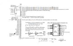
If you have a desoldering station/unit and the correct IC socket. Carefully remove the E104 chip and solder in the socket.
Once you have done this you could temporary wire (jumper) the un-inverted A16, A17 and A18 inputs to the chips output pins for A16I, A17I, A18I. In this cast , bi passing the 74Ls138 inverting the outputs of address
pins A16,A17,A18. If the memory Card now works then memory bank addressing is some what different. On some memory expansion Cards the Address block decoding is done in a PLA gate array. This could also be
a issue to deal with depending on how it is coded.
..
Other possible issues :
100A and or 100+ Motherboard layout does not matches the one I attached.
Newer BIOS firmware in the 100A that has a 384K ram limited on it.
Some Io cards that use the 100A Memory expansion Bus connector use the NONSHRCYC signal. But it look like you don not have any, so I omitted it for now.
On the memory expansion connector the undocumented ghost pin 5 could be in affect on your system, so you might also have to play around with it as well.
The memory card could also be overlaying the 100A, 100+ System Boot memory Block, The Video memory Location, depending on how the did the address decoding logic.
On the 100A and plus models the PLA chip that generates the NONSHRCYC or Share memory cycle could also come into effect if its coding was changed from the original version and there other (undocumented)
differences in the motherboard.
..
Depending on whos and how the memory Expansion card was designed, you might have to patch up the memory expansion card to work at the first memory block above 64K. Basically any address with A16 active
(and likely in it is none inverted form). The first 0-64K is onboard memory in the 100A, 100+ and on the 100B its form 0K- to 128K. (Most likely a undocumented change in the Memory cards PLA so it won't work).
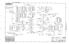
There was a reason that I included the 100B Memory expansion unit schematic that uses a PLA. Mostly for bug hunting reasons and incase you have to do some hard wire some jumpers on the memory Expansion
Card as well.
..
If the RAINBOW 100A or + model will boot to command level with the card install, this is good site to see, because the memory expansion is not interfering with the Base memory on board.
You can then run the Memory Test utility form the Diagnostic diskette, to test the memory Expansion unit out.
Once the memory expansion unit is working but the system under MS-DOS only see part of the memory, then you will likely have to patch MS-DOS as well.
..
Hopefully one of these Fixes the memory expansion bugs.
 
Last edited:
Hi there -- I found time today to try out the initial mods to get the 100A to 512k. Sadly, I've not been able to get it working yet. I've re-routed the IO/M signal to header pin 30 (I have continuity back to the 8088) and connected pin 11 on E104 to header pin 43, removing the connection to pin 12. The trace to header pin 30 is on an inner plane so I had to hunt for vias -- I found one trace route (which is where I connected the IO/M signal) and cut the trace outboard of my new connection, but perhaps there are other parts of the circuit I haven't disconnected yet.

In any case, I simply get a hung system on powerup. I've tried grounding connector pin 29 on the 100B card (no change) and tried various combinations of the dip switch settings on the 100B card (also no difference). I will hunt down the LED codes when I get a chance (I either get leds 1-3 solid on, or all leds solid on). I was unable to find any connections to pin 29 on either my 100B card or on na103's schematics for their revised 100B adapter. So perhaps I've missed something there. (My 100B card is a stock DEC one, currently fully populated with 3 banks of 256k)

The 100B card is tested good in a 100B rainbow that I have. The 100A rainbow works fine with and without a 100A expansion card. Perhaps my machine is of a revision that doesn't work with this mod, or perhaps there's a ROM version issue (I thought mine had the latest but I'm not 100% sure). Perhaps A19 needs to be connected differently for it to work? Or perhaps there are additional firmware steps needed. Or perhaps I've just messed something up lol, which is entirely possible. I will review my changes when I get a chance, not able to work on it for a short while.

Any thoughts welcome!

Cheers, A
I was kind of busy until today to reply.
So we are dealing with a 768K real DEC Made Memory Expansion Unit that helps clarify what we are dealing with.
As far as all the LED status indicators as on. Main Board [rom crc, rom 0] address from FAOOO to FC000 on the 100A and + models.
Interrupts Off* ................................................ xxxoooo
Memory Board [ram option] ................... ---xxoo
Main Board [ram arbitration] ................... xxxoxoo
Main Board [nvm data] .............................. xxxxoxx
Main Board [unsolicited interrupt, Z80] xxxooox
..
Sorry but I don not have 100A expansion card or the na103's schematics for their revised 100B adapter board. There could be a undocumented incompatibility issue here.
No pin 29 used on your 100B (memory expansion Card) No Memory Option Present signal - This will be a big issue - So I will have to ask when was the card made and what is is its full part number.
On our Old 100B model if there is no active Positive or active Negative memory signal on pin 29 then it will not see any memory card that installed. Yes I have seen some cards that overlay the expanded memory
detected bit in the systems registry for it. These ones case a lot of problems if you have other peripheral cards that use that bus connector as well.
..
Does the 100A have the hardware patch for the secondary interrupt Table (vector address) installer, since we are getting the Interrupts Off* I wonder if that fixed was installed or not. This is where they wire the 8251 USART pin 24
the /DTR signal back into the chip that generates the INTL signal on its Data bit 5 pin. Even if this was done I have a lot of software for the model B and on worn out diskettes cause this error.
..
Does you 100A or plus model have the adapter board to use 100B Firmware ROMS. There could be a issue their.
..
Hopefully you are not trying to do this on a 100A, 100+ with a DEC's memory Adapter card or DEC's 8087 NPU adapter installed. Some versions if this adapter card changes some of the systems hardware registers.
They already have the logic for extra memory, So I don't think where are trying to repeat it. But maybe we anciently are if they are installed. Since this wasn't noted (aka messaged about, I was assumed as not installed).
..
It has been quite a while since I did hardware work (or make replacement for the RAINBOW 100 computer system.
With A19 low and A16, A17, A18 all high that is only the address of 229376 dec 38000 in Hexdec., or in binary 0111000000000000000
With a 19 also high I think the address some thing like 491520 dec 78000 in Hexdec., or in binary 1111000000000000000
? what overlay is causing the Main Board [rom crc, rom 0] on the 100A or + models is causing this error. Something could be addressing a model B firmware address !
..
Could be a compatibly issue using a none 100A memory card slot based expansion card with this adaptation.
Well that is all for now,
 
Hi!

Thank you for the comprehensive reply! (I very much appreciate it)

I agree that it might be best to socket E104 and go from there, so that's what I will likely do -- I do have some desoldering experience BUT I find with (well made and thick) boards like IBMs etc getting enough heat into the area without causing damage is a challenge, so I'll need to figure out how I want to approach this.

So, prior to that... information gathering!

1) I've attached photos of the 100B memory expansion card I'm using. Part number is 5015960-01-C1 or 5415961 (not sure which number is part #). Don't mind the dip switch settings, I was trying options. (note that with switch 4 OFF, I get to a "Z80 crc error" message rather than a full hang). Perhaps this is simply a 100B card that will not work with the 100A?

2) I am using what seems to me to be a fully stock 100A board (not 100+) without any memory adapter other than the 100A expansion card that was installed when I purchased the system. The BIOS version on my board is 4.03.11A which, from what I gather (see http://oldpc.su/articles/dec_roms/) is the latest available for the 100A (3 roms, no evidence of a 100B ROM adapter). I imagine these are 23-176E4, 23-177E4 system ROMS and the third being either the language or chargen rom (not sure))

3) As far as updates or modifications to the mainboard, I haven't seen any evidence of rework (bodge wires, additional components). I can provide photos of the front and back of the mainboard if it would be useful. (I'm not sure of the location of the 8251 USART you mention, but I can take a look).

Unless any of this information proves to be a show-stopper, I will work on socketing E104.

Cheers and thank you again! A
 

Attachments

  • Rainbow100BMemExpBack.jpg
    Rainbow100BMemExpBack.jpg
    3.9 MB · Views: 5
  • Rainbow100BMemExpFront.jpg
    Rainbow100BMemExpFront.jpg
    1.7 MB · Views: 5
Oh, the bodge wire on the back of the 100B expansion card was me grounding pin 29. As I mentioned before, I wasn't able to find anything on the board pin 29 was connected to, which seemed odd to me -- I was expecting some kind of pull-up resistor type connection to enforce logic high. It may well be there and I just haven't found it, in which case this could be causing a conflict on the pin 29 signal and hence the whole problem :)
 
Thanks for sending the data about your system and the pictures that help clarify what we are dealing with.
Hopefully I get enough free time to check you firmware version against my RB100 models still in service. But anyways lets continue with the issue at hand now.
..
Ya the missing Signal from pin 29 could have been done on purpose since the latest soldered component date is from 1985 and the rest are from 1984.
You should try to make sure pin 5 on the E104 chip is pulled low (maybe gnd it if it us un connected) as this is the IO//M input to the chip to disable it.
In side the model 100A and or + models they use a pull up resistor where the register latch is located for the Memory Card Detection register.
If you want to try to force the 100A into thinking it has a expanded memory allays attached you could try to connect that registers data bit to ground, directly.
In this case it would be IC E59 a 74LS244 on Pin 2 that has the Memory Pres L signal is inputted to read only register at IO address #2 (hex?)
This signal has a pullup resistor on the 100A mother board connected to +5V dc.
..
The socketed DM74S287N on the memory expansion card next to the dip switches could be the bug, its a (256 x 4) 1024-BIT TTL PROM.
The DIP switches select wither each ram bank contains 64K or 256K DRAM chips and the only other thing the dipswitch does is disable the parity memory.
Dip Switch setting 1 is for Party checking or No parity Checking on older board versions. The rest relate to the DRAM chips used in the banks.
Bank 1 is the outmost away from the memory expansion connector, and of course bank 3 is the closest to it.
..
The other thing you could try is to temporary connect A19 to +5V dc on the memory card and make sure on the system side that pin has been disconnected from ground.
If the computer now sees the memory card then in some time DEC changed the bank addressing code in the address mapping PROM on the memory expansion card.
Of course were scrambling the memory map a bit more. (Relocation the Memory Bank Address by re routing the address lines).

If you have some spare power diodes you could also try to check pin 34 on the Memory Expansion Connector , for feed back.
This is the INIT Low Signal Initialize. You might want to try a diode to make it read only access on the memory card. But I don't think this is a issue.
If the system was booting, we would get errors when the system try to refresh those status registers on the motherboard, and where not getting that far.
..
We used mostly 3RD parity 896K or 832K Memory expansion boards that work in ether model, most of then used a kitty chip socked for the connection to the E104 chip.
..
I have included the data sheet for the 54S287 prom. you should check this PROMS pinout on memory expansion board with the one on the hand drawn version I original attached
to a older message. Their should be 2 signal lines tied to GND other then the chips power supply and pin 9 the q3 signal should be unconnected. (if its different ? their has been
a change in the board design).
..
There is a bit more I can Add, But I see how this works out first. I would also re check the circuit traces back out for errors.
The model B adapter ROM board for the model A or Plus models was none a DEC item, nor was the ESDI or SCSI or Priam Hard disk Controller card, The IEEE-488 Card,
Lab Bus I/F card, The ISA-Bus Adapter, the original ethernet card, the Parallel port card, the Coruvs network cards. and there where several others.
..
The strange rom error that you encountered. As far as all the LED status indicators as on. Main Board [rom crc, rom 0] address from FAOOO to FC000 on the 100A and + models.
that address starts @ 1024000 dec. in binary it is 11111010000000000000. That is A19 back down to A0. Could be a undocumented firmware bug with the memory expansion card.
There is likely an undocumented bug/change some ware that is causing a snag with a newer version of the memory expansion card. (Likely the Prom on card)
..
Since you where getting a Interrupts turned Off error, there could be other issues that we should maybe look at as well.
You should do the secondary vector memory circuit patch if you are getting a lots of Interrupts turn off errors running software written for the Model B that runs fine on a real model
B without the error.
..
But I would not be surprised if some one at DEC did some changes to stop the 100B cards from being adapted to the model A and/or + models .
Hopefully we are not looking at that with DEC, but perhaps this is simply a (newer/revised) 100B card that will not work with the 100A.
IBM did this with the 5100 series computer line against Core Designs many years ago and with others on the IBM System 23 and Displaywriter (6580) systems.
..
I will now wait for your next reply to see where we our progress go from there.
Thanks'
 

Attachments

  • DM54S287.PDF
    133.8 KB · Views: 2
  • DecRB100 MemorytestDOC.pdf
    299.8 KB · Views: 4
Last edited:
Hi,
I'm joining this interesting brainstorming by adding some information about the DM74S287N PROM.
in my remake it was replaced with a more modern GAL.
to do this I had to reconstruct the truth table based on the specifications of the manual.
the memory banks of the option ram are activated or deactivated based on the addressing. the memory range is from 0x20000 to 0xDFFFF.
pins A16 to A18 are used to address this range.
1712653383949.png
from the schematics of the rainbow 100 A it doesn't seem to me that A16 - A19 reach the Option RAM in any way.
it would be interesting to be able to build a expansion that somehow works without modifying the mainboard.
This article reports that Jerry Miller of Suitable Solution has designed a 100A memory expansion called RAMbow (a funny name) that kick memory to 896k without the need for adapters.
 

Attachments

  • RAMbow.pdf
    1 MB · Views: 6
Is my opinion that RAMbow could be an all-in-one board consisting of the memory card + 8087 adapter.
in the article it says that it was sold fully populated with nine one-megabit chips.
This creates space on board to place the CPU socket and any other logic.
At the moment I'm busy with other projects but it shouldn't be a problem to design a new board with these specifications starting from my work on the PC100 for the 100B
 
Hi na103! I'm glad you're joining the discussion, the more the better :)

If you ask me, a modern re-engineering of the Rambow (lol) would be amazing. The only thing, it seems to me, that really limits the 100A is the memory size, and the only thing causing that is a scarcity of the OG solutions like the original "8087" memory expansion card. Please, go for it, and happy to help in any way!

As far as the dip switch settings on the 100B card go, na103 you indicate that switches 1-3 are used for banks 1-3 activation, whereas N. Brown earlier indicated that switch 1 was parity on/off and 2-4 were banks 1-3 on/off, if I'm understanding correctly. Is this a difference in your re-engineered card, or were there simply variations in the original designs? Do we know? I don't know if the card I'm using is the same original card as what you were using for your reverse engineering.

N.Brown -- I wouldn't mind trying out the mod you indicated: "wire the 8251 USART pin 24 the /DTR signal back into the chip that generates the INTL signal on its Data bit 5 pin" as being a simple non-destructive mod. Do you happen to know on the chip placement diagram which two chips these are? I wasn't sure (wow if we had full schematics of the 100A it would be VERY handy). I also think socketing E104 is a good plan, as also being non-destructive (If I don't mess it up lol).

N.Brown -- thank you for the huge amount of information; I'm still digesting it. What I think I'd like to try is:

1) Try to confirm the dip switch settings if we can
2) Do the 8251 mod
3) Socket E104
4) connect A16-A18 directly to the memory expansion rather than inverted
5) connect A19 if step 4 works (or perhaps even if it doesn't) -- or try just pulling it high as you suggest.
6) put everything back to stock and use na103s re-engineered solution! (which yes would be, as I said, AMAZING to have in the world).

Let me know if this seems sensible, or if I've missed something?

Cheers all! A
 
Hi,
I'm joining this interesting brainstorming by adding some information about the DM74S287N PROM.
in my remake it was replaced with a more modern GAL.
to do this I had to reconstruct the truth table based on the specifications of the manual.
the memory banks of the option ram are activated or deactivated based on the addressing. the memory range is from 0x20000 to 0xDFFFF.
pins A16 to A18 are used to address this range.
View attachment 1277617
from the schematics of the rainbow 100 A it doesn't seem to me that A16 - A19 reach the Option RAM in any way.
it would be interesting to be able to build a expansion that somehow works without modifying the mainboard.
This article reports that Jerry Miller of Suitable Solution has designed a 100A memory expansion called RAMbow (a funny name) that kick memory to 896k without the need for adapters.
Thanks for joint this ongoing brainstorm memory expansion communications for the Rainbow 100A and plus models.
Ya the Suitable Solution did a flew boards for this machine. And thanks for digging up a review for the old RAMbow memory expansion card.
Personal I have never cane accessed one to work with, but I would like to get a hold of the units schematics and a couple of pictures of it.
The dip switches are in a different order then in my old DEC manuals, but it looks like only the Party control Switch has changed position with what is on other documentation.
..
If Address A16 to A19 don not reach the Option Ram how can the card address more then 64K with out using bank switching. Even if they are using the Shared/Noshared signal
that only really gives another 64K on a machine with a maximum address line of A15. Some how the A16-A19 signals have to be directed to the cards memory bank block selection unit.
They are there on the model 100A and or the + model memory expansion connector but are inverted other then the A18 signal and the deleted A19 signal.
NONSHRCYC or Share memory=Shared/Noshared listed above.
 
Last edited:
Hi all -- I have the 100A board back out and will try to solder in the socket tomorrow (it's Tuesday night here now, Toronto Canada). I will also take pics of my motherboard and I will take pics of the 100A memory adapter. I will also see if I can trace continuity from E104 pins 12-14 through the J6 connector and find out where the A16-A18 inverted signals go on the memory expansion card (I'm assuming, like N.Brown, that they do, and are used for bank switching).

Cheers! A
 
Back
Top