• Please review our updated Terms and Rules here

Rainbow 100A Memory beyond 256K?

however this does not matter for RAMbow.
I can eliminate E29 and manage the addressing with a GAL logic and a jumper to set when RAMbow is installed on 100A or 100B.
The E27 multiplexer is also useless as it is only needed if you intend to use the 100A's memory card on the 100B.
There's probably no point in using RAMbow on the 100B when you can use its memory card.
Anyway this is the outline of what I think RAMbow might look like.
I'm waiting for some of your comments and suggestions.
Thank you
I have looked at your bate/rough outline board their is a couple of things I would have done differently.
There is no MMU logic on it to properly decode the upper address range, you could always wire this bank into an I/O address ranger to select it this will stop conflicts with the systems design,
and the Intel 8088's required boot up memory block. Of course with additional logic this area can also be made useful. (see my next entry for more information).
..
I would add a bit of logic so it will work with both models, The jumper you have done, and I would connect it to the memory expansion bus memory present signal as well.
This would free up the memory expansion slot for other peripherals. Do to the space restrictions you can only double stack 2 cards if the card has the through connector for it.
I would also properly implement the Shared/None Shard signal as well. You have the extra unused signal pins on the E20 GLA chip to help do so.
..
It cool to see that you went right to 9-bit refresh in the refresh counter circuity.
from what I've seen when a 100B memory is installed via the 8087 adapter on the Rainbow 100A, MEM PRES remains high.
this means that the logic does not detect the presence of the extension memory and I think that even the BIOS memory set-up settings in 100A become irrelevant.
at this point all the signals (S64K 1-3 and NONSHRCY) are no longer important for external memory access purposes. the only thing that matters is addressing and IO/M
 
Last edited:
from what I've seen when a 100B memory is installed via the 8087 adapter on the Rainbow 100A, MEM PRES remains high.
this means that the logic does not detect the presence of the extension memory and I think that even the BIOS memory set-up settings in 100A become irrelevant.
at this point all the signals (S64K 1-3 and NONSHRCY) are no longer important for external memory access purposes. the only thing that matters is addressing and IO/M
Ya the BIOS memory set-up settings in 100A become irrelevant when a 100B memory is installed via the 8087 adapter on the Rainbow 100A and the MEM PRES remains high.
But I I have already noted that I have other none memory expansion cards for the 100A that use the Memory Expansion Connector. So I will leave it at that for now.
 
I did not read through the whole thread - but I got the impression that no complete circuit diagrams of the adapter exist ?

Many years ago I inherited a pile of paper copies from a former collegue who worked in the DEC repair center
There are some diagrams of this PC100A 8087/Memory adapter module

As I have no A3 scanner, I took camera pictures and tried to convert them into a somewhat clean PDF format

I hope I can upload them here in a good quality, due to size restrictions

Are there any other missing diagrams of the PC100 ?
i.e. the Power supply ?
 

Attachments

  • PC100A MA Dwg 2.pdf
    5.8 MB · Views: 16
I did not read through the whole thread - but I got the impression that no complete circuit diagrams of the adapter exist ?

Many years ago I inherited a pile of paper copies from a former collegue who worked in the DEC repair center
There are some diagrams of this PC100A 8087/Memory adapter module

As I have no A3 scanner, I took camera pictures and tried to convert them into a somewhat clean PDF format

I hope I can upload them here in a good quality, due to size restrictions

Are there any other missing diagrams of the PC100 ?
i.e. the Power supply ?
Hi Guenter,
once again you save the day.
thank you, thank you so much for these schematics.
now I have a few nights to spend awake working on the 8087 adapter.
send picture of everything you find!
Regards
Nicola
 
I did not read through the whole thread - but I got the impression that no complete circuit diagrams of the adapter exist ?

Many years ago I inherited a pile of paper copies from a former collegue who worked in the DEC repair center
There are some diagrams of this PC100A 8087/Memory adapter module

As I have no A3 scanner, I took camera pictures and tried to convert them into a somewhat clean PDF format

I hope I can upload them here in a good quality, due to size restrictions

Are there any other missing diagrams of the PC100 ?
i.e. the Power supply ?
Right On another missing schematic diagram has been found, No more manually redrawing out the PC100A 8087/Memory adapter module with all the IC Installed.
This should help speed up NA103 progress and other who want to recreate that adapter.
..
As NA103 states send picture of everything you find! as some of the online archives for this system are incomplete any additional data will help.
..
The original DEC. RB100A schematics for the model A original memory expansion unit is also missing online as well.
..
 
Due to (PDF) size restrictions with this host for uploading files , you could try the https://www.ilovepdf.com/compress_pdf online utilities.
Some other PDF software from none Adobe will let you save the PDF as an older version thus reducing its file size as well.
In some cases the PDF in it is really large, you still might have to split in into several small parts, then upload them , to get around the size restriction).
..
I Don't know if this message is of any help. I If not just ignore it them.
 
Aileen Rainbow 100 hardware
Dec. supposed to designed a Ethernet board for the RB100 computer as well.
If you Dec. Documentation has ant 3RD parity cards for the RB100 computer that would be interesting as well.
..
Well that is all for now.
 
What I found in the pile of paper - mostly multiple paper copies in mixed quality

PC100 Motherboard 54-15486-01
PC100B Motherboard 54-16206-01

PC100B Memory Extension

H7842D PSU Test procedure/Specs
H7842 PSU Circuit Diagrams

VT100 Monitor board

No other "interesting" stuff so far

Just searched the Web for PC100 Circuit diagrams
It looks like
PC100 Motherboard 54-15486-01
PC100B Motherboard 54-16206-01
are well covered on bitsavers.org
So I will upload the other mentioned diagrams only - give me some time

As this is quite some work for me - what is really urgent/required ?

Where can I upload larger files in an easy fashion ?

BR Guenter
 
Last edited:
What I found in the pile of paper - mostly multiple paper copies in mixed quality

PC100 Motherboard 54-15486-01
PC100B Motherboard 54-16206-01

PC100B Memory Extension

H7842D PSU Test procedure/Specs
H7842 PSU Circuit Diagrams

VT100 Monitor board

No other "interesting" stuff so far

As this is quite some work for me - what is really urgent/required ?

Where can I deposit larger files in an easy fashion ?

BR Guenter
the motherboards rev A and B, vt100 are already present in the bisavers archive.
PC100B memory extension is in my repo github and also here somewhere in the forum.
of the PSU I think there is only reverse engineering by Tony Duell. so it's all interesting.
obviously nothing is urgent in these cases. ;-)
the right place to save documents would be bitsavers.org but I can also host something in my github repo.
or even here in the forum it could be fine.
again thank you so much for this

Nicola
 
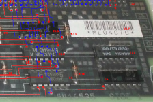
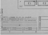
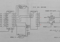
there is something strange that I don't understand.:unsure:
IC E5, E6, E11 and E17 are present in the part list.
However, they are not present in the schematic and a note on the layout sheet says that they are spare.
I checked in the pictures of N.BROWN, E17 is not there but the others are present and connected in some way to the other ICs
for example pins 9 and 10 of E5 are connected to pins 13 and 9 of E1
1714031847365.png1714031883601.png1714032285962.png
 
there is something strange that I don't understand.:unsure:
IC E5, E6, E11 and E17 are present in the part list.
However, they are not present in the schematic and a note on the layout sheet says that they are spare.
I checked in the pictures of N.BROWN, E17 is not there but the others are present and connected in some way to the other ICs
for example pins 9 and 10 of E5 are connected to pins 13 and 9 of E1
View attachment 1278550View attachment 1278551View attachment 1278552
 
The Memory Adapter with the optional 8087 Option pictures I originally uploaded, could be different then the
ones that BIGFIX provided in there uploaded documentation. Some boards have a 541634-X-X-cX number.
..
For those forum users that are following this set of messages just so you know that the file pc100a-ma-dwg-2-pdf, contains two
circuit schematic diagrams but only one component layout for both schematics.
..
The Memory Adapter with out the 8087 NPU option on board should use fewer logic gates then the one with the 8087 NPU installed.
A part number with a C1 is without the 8087 installed and a C2 has the 8087 installed.
..
The document that user BigFix upload is Documentation Number 546535-0-0BP2 rev A with dates form 04-Apr-1984 and the release date of 15-June-1984. If you look at page 1 of this documentation you will see that there has been some revisions. The Etched Circuit Board is listed as a rev. B1 and is for DEC. PN 5016534-01 but the PCB component layout is (UA) 5416535-0-0A that this file contains.
..
It could be some thing like this:
As far as IC E5, E6, E11 and E17 are present in the part list but are not on the schematic likely means a different PCB board with a different circuity being used. When DEC originally designed the Rainbow 100 computer they put the Intel 8088 that is on its motherboard in Minimum Mode. To use the 8087 NPU/FPU/APU in minimum mode and/or with a Z80 microprocessor will take some extra support logic to work.
..
Dec part # 9009185-00 is not used but it was still noted in the part list.
E5 is an 74F08 AND gate Quad
E6 is a 74F00 NAND gate Quad
E11 is a 74LS74 FF-D Dual Edge Triggered.
E17 is unknown
..
As far as extra logic gates. (Some 3 RD parity NPU adapter boards also do this as well)
There was likely hardware wired on the board so MS-DOS would automatically detect the NPU as being available (regardless of what the BIOS states about it). You would have to look up the memory location that older versions of MS-DOS check for it. (Likely, some where in the private memory spaces IO Vector and its relocation table addressing).
..
Other possible issues.
Print Errors in the documentation for DEC, there also could be other versions of the board out there that there is no current data
available for it.
..
You might have to manually compare BIGFIXs schematics with the Component layout that is with it and delete the unused logic devices
on a copy of there set. This would let you confirm what you are looking at. You could also try to directly bread board a evaluation unit off those schematics and then test it.
..
 
1) Try to confirm the dip switch settings, the NA103 card is different then in the manual I attached I attached in a previous message.
In theory of the 100B model you should bet a error message about party error checking with either the first switch 1 or the last switch. Then you might have to go through both schematics to verify which one closest matches yours.
In the list above you forgot about the IO//M signal line replacing the Shared/noshared signal at the memory expansion connector on the 100A.
If your number 4) fails try pulling A19 high, then if nothing try pulling A17 alone on the memory expansion card high. This will change the memory origination on the card.
..
On the Rb100A_component layout
IC E87 a 8251A USART chip pin 24 the DTR signal to pin 8 IC e72 a 74LS244 on the D3 input line which should outputted on pin 12 as BAD3 signal. Of course you must cut the ground signal connected to pin8 of IC e72.
This modification should be available some here on the internet, if it hasten be removed.
..
6) might be your end solution , but a couple years ago I did try to contact the author directly at github.com for the RB100A version of the memory expansion card. but never got a reply.
It was probably got marked as Spam or something like that.
..
Sorry to put you through this, but the old version of the card we where able to modify for use with the 100A and or plus models at one time, including versions that did not have the PLA on board.
A durity /hard to read copy of the RB100A schematics can be found @ http://www.bitsavers.org/pdf/dec/rainbow/MP-01491-00_PC100_Print_Set_198212.pdf
(If I you mess it up lot, please let me know as I still have 3 extra RB100A models sitting around as part units for on going maintenance contracts, since I open up my big mouth in the first place. ).
..
The Modify Int.. Vector is not the same one that used to modify the 100A to a 100B Level.
For this revision I can longer find the modified BIOS ROM of the Darkweb for it.
 
The Memory Adapter with the optional 8087 Option pictures I originally uploaded, could be different then the
ones that BIGFIX provided in there uploaded documentation. Some boards have a 541634-X-X-cX number.
..
For those forum users that are following this set of messages just so you know that the file pc100a-ma-dwg-2-pdf, contains two
circuit schematic diagrams but only one component layout for both schematics.
..
The Memory Adapter with out the 8087 NPU option on board should use fewer logic gates then the one with the 8087 NPU installed.
A part number with a C1 is without the 8087 installed and a C2 has the 8087 installed.
..
The document that user BigFix upload is Documentation Number 546535-0-0BP2 rev A with dates form 04-Apr-1984 and the release date of 15-June-1984. If you look at page 1 of this documentation you will see that there has been some revisions. The Etched Circuit Board is listed as a rev. B1 and is for DEC. PN 5016534-01 but the PCB component layout is (UA) 5416535-0-0A that this file contains.
..
It could be some thing like this:
As far as IC E5, E6, E11 and E17 are present in the part list but are not on the schematic likely means a different PCB board with a different circuity being used. When DEC originally designed the Rainbow 100 computer they put the Intel 8088 that is on its motherboard in Minimum Mode. To use the 8087 NPU/FPU/APU in minimum mode and/or with a Z80 microprocessor will take some extra support logic to work.
..
Dec part # 9009185-00 is not used but it was still noted in the part list.
E5 is an 74F08 AND gate Quad
E6 is a 74F00 NAND gate Quad
E11 is a 74LS74 FF-D Dual Edge Triggered.
E17 is unknown
..
As far as extra logic gates. (Some 3 RD parity NPU adapter boards also do this as well)
There was likely hardware wired on the board so MS-DOS would automatically detect the NPU as being available (regardless of what the BIOS states about it). You would have to look up the memory location that older versions of MS-DOS check for it. (Likely, some where in the private memory spaces IO Vector and its relocation table addressing).
..
Other possible issues.
Print Errors in the documentation for DEC, there also could be other versions of the board out there that there is no current data
available for it.
..
You might have to manually compare BIGFIXs schematics with the Component layout that is with it and delete the unused logic devices
on a copy of there set. This would let you confirm what you are looking at. You could also try to directly bread board a evaluation unit off those schematics and then test it.
..
The standard IBM PC and PCXT use the following addresses for the NPU addressing (in Hex format)
0F0 Clears Math Coprocessor Busy Signal
0F1 Resets Math Coprocessor
---------------------------------------
0F2 reserved
0F3 reserved
0F4 reserved
0F5 reserved
0F6 reserved
0F7 reserved
* 0F8 to 0FF Math coprocessor Addressing
---------------------------------------
0F8 Opcode Write to NPU, Read CW or SW register from NPU
0F9 Reserved for upper byte access in 8 bit systems
OFA Write Data to NPU or READ data from NPU
OFB Reserved for upper byte data access in 8 bit systems
OFC Write Exception Pointers or Read Exception Pointers (for none Intel)
OFD Reserved for upper byte access of Exception Pointers in 8 bit systems
OFE Read Opcode Status All or Write Opcode Status (for none Intel)
OFF Reserved for upper byte access of Opcode Status access in 8 bit systems
============================================================================
..
IBM 5155 5160 PCXT models register address coinsuring NMI signal use (In hex).
Port Address:
62 input Bit 1 +CoProcessor Installed
===== Bit 6 + I/O Channel Check
===== Bit 7 +RAM Parity Check
61 Out Bit 4 -Enable RAM Pariy Check
==== Bit 5 -Enable I/O Channel Check
==== Bit 6 -Hold Keyboard Clock Low
==== Bit 7 - Enable Keyboard or + Clear Keyboard
..
A0 to AF NMI Mask Control Register (XT only)
that is from 160 in dec. or 10100000 in binary to 175 in dec. or in binary as 10101111.
..
IBM PCXT System BIOS 8088 Software Interrupts theats a NMI interrupt like this :
Int. 02 Address 8B NonMaskable uses BIOS Entry of NMI_Int. So on systems that have no 8087 routeteens in the BIOS firmware
they are hard coding the 8087 interrupt in logic circuits.
..
The DEC. Rainbow 100 Computer uses those address (61,62, and A0 to AF) above for different hardware.
Might have to dissemble a newer version of Cold Blue for the Rainbow 100 computer and the MS-DOS 2.00 support utilities for the
computers 8087 to get the Vector table location for the 8087 and its data bit used, if all else fails.
..
Hopefully this messages help explain what pins 13 and 9 of IC 1 the I/O QA decoder circuit are used for that is not shown on the schematic provided by BIGFIX.
 
Last edited:
Back
Top