• Please review our updated Terms and Rules here

Vectrex (newer version - no buzz) - Troubleshooting Sound but no Video

miata

Experienced Member
Joined
Sep 18, 2019
Messages
197
Location
Dresden, Germany
Hi Vectrex experts,

i found another Vectrex but unfortunately it is not happy 😳 Similar to my other one (before Daver2 helped me to fix it) I can hear the gameplay but there are no vectors on the screen. I can see the neck of the tube glowing so I still have some hope to fix it. I did the first checks on my own as Dave has teached me ( thanks again, Dave):

- Power from the transformer is at 10,5 VAC on both lines, ok
- I can measure +5VDC, -5VDC, -13VDC at the analog and digital board in a good range
- I also find the supply voltages on the various chips at the digital board, they look ok too
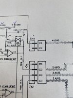
- I replaced already IC207, IC301, 302 and 303 taken from my other Vectrex- obviously no issue here
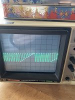
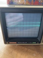
- I used my scope to look to the X,Y and Z waveforms and they look all good on both boards and according the manual

However I found these issues:
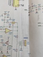
1. I checked the voltages at the CRT PCB and they look ok apart from EP505, here I measure -9,25VDC which looks off
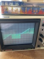
2. At IC302-14 I get a flatline with my scope instead of a waveform
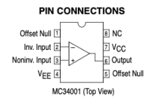
3. Very strange are the voltages on both Pots R333 and R335, I measure -5VDC on all 3 pins on each Pot independent what is the position of adjustment. Actually and according to my other Vectrex there should be +5VDC on one side and -5VDC on the other and then with the pot the voltage will be adjusted I assume. Something is not right here!

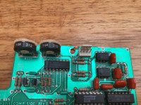
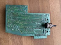
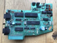
I decided to follow up the last issue first and de- installed the digital board. Looks like that all 3 Pins on R333 and R335 are connected to IC 304 or IC306. Maybe one of these chips or even both are faulty?
Unfortunately my schematic does not fit to my hardware although it says its for Revision 3GE like on the sticker on my digital board. There is no IC306 in my schematic but on the board 😳 A bit difficult to check what is going on here.

Is there anybody able to help me?

thanks
best regards
Denis
 

Attachments

  • 1FF02B76-5FFA-4EAC-B56C-682609B177B7.jpeg
    1FF02B76-5FFA-4EAC-B56C-682609B177B7.jpeg
    2.1 MB · Views: 11
Last edited:
Of course there is Denis!

Although I wouldn't call myself an expert...

Just been doing another job and got home. Let me have a look shortly...

Dave
 
I only have the 'old' schematic to hand also. The only slight difference is the OPAMP packages that are used. We can work through that though.

The -5V at the power connector is used as the analogue -5V (-5V ANA); and this seems to be present.

The +5V is used as both digital +5V (+5V DIG) and analogue +5V (+5V ANA). They are sourced from the same power line/pin but they are completely separate PCB tracks. It sounds like there is a PCB track break somewhere in the +5V ANA network.

Can you measure the voltages on pins 7 and 16 of IC302 (4052B) please and report back.

It would also help to look to see if any of the PCB tracks are damaged - or even burnt.

Can I also suggest downloading the datasheets for the OPAMP ICs, identifying the positive and negative power pins and measuring them.

The OPAMPs should be fed from +5V ANA and -5V ANA, and these are the power pins that the two extreme 'ends' of potentiometers R333 and R335 should be connected to.

If +5V ANA was open circuit, this would account for why there was -5V on all pins of the potentiometers R333 and R335.

Dave
 
Hi Dave. Here we are again 😊🖖 thanks for your quick response. I appreciate.
I will look in your advice tomorrow as I am out with friends tonight.
 
Good Morning. So I went through the tasks:

1.) Can you measure the voltages on pins 7 and 16 of IC302 (4052B) please and report back
I cannot right now as I de- installed the board for further troubleshooting but I am sure I also measured good voltages on these pins when I went through the several chips to measure their supply voltages. Just looked for continuity and I can clearly see that both pins are connected to +5VDC ANA andd -5VDC ANA
That also confirmes there is no crack on the board for these lines

2.) Can I also suggest downloading the datasheets for the OPAMP ICs, identifying the positive and negative power pins and measuring them.
Confirmed! I have checked that also before. I clearly found +5V at Pin 7 and -5V at Pin 4 when I did my measurements days ago. Please find attached the pinout. However I dont understand the circuit and why there is 2x Offset Null being used.

3)The OPAMPs should be fed from +5V ANA and -5V ANA, and these are the power pins that the two extreme 'ends' of potentiometers R333 and R335 should be connected to.
I can confirm that -5V ANA is connected to the supply as I see the direct connection to C317. Continuity is perfect.
I dont understand how the +5V ANA is provided to R333 and R335. I did not find any direct connection nor I was able to measure continuity for this line from somewhere. It seems the +5V ANA is provided through IC304 and IC306?

Please see attached photos. I marked one up to highlight how the Pots are connected. Would like to understand how the +5VDC ANA is going to them. Cannot see any other trace from the Pot´s to somewhere else at the board other than to IC304, IC306 and the -5VDC supply. However I measured continuity between the various colored pins and it is all ok.

fullsizeoutput_280c.jpeg
 

Attachments

  • MC34001P Pinout.png
    MC34001P Pinout.png
    15.7 KB · Views: 7
  • ewYzjFOfQryaME2SDih84Q.jpg
    ewYzjFOfQryaME2SDih84Q.jpg
    2.4 MB · Views: 7
  • fullsizeoutput_280f.jpeg
    fullsizeoutput_280f.jpeg
    4.6 MB · Views: 5
Last edited:
Excellent detective work. Your post has just caused a neuron to fire now regarding the offset null...

Ignore the +5V ANA and -5V ANA rubbish...

In the 'older' design they used a LF347 quad OPAMP package. In order to compensate for the inaccuracies in the OPAMP they use a potentiometer bridging +5V ANA and -5V ANA with the wiper of the potentiometer being fed to the inverting input of the respective OPAMP where the signal is summed with the other (dynamic) input.

The newer circuit (with the MC34001P) has one OPAMP per package, but this device has in-built circuitry for the offset null input. In this mode, -5V ANA is fed to the WIPER of the potentiometer, and the two 'ends' are connected to dedicated pins on the OPAMP. As a result, you will NOT see the voltage swings on the new circuit in the same way as the old circuit.

I therefore suspect that this is a red herring (as we say in English).

Let me see if I can find the 'correct' schematic....

A quick question: are you using the diagnostic cartridge or a game (e.g. minestorms) for your testing?

Just to confirm: when you were doing your testing you saw 'sensible' X, Y and Z signals at the connector between the digital and analogue boards? I assume the X and Y signals were being driven both driven positive and negative? What about the Z signal? What was the highest and lowest voltage it was switching between?

Dave
 
Last edited:
Hi Dave. Thanks for the clarification. So the thing with the R333 and R335 is actually a „non issue“ as my US colleagues like to say but „red herring“ describes it much better 😊

Please see attached the photos what I have taken when I scoped the X,Y and Z. They look quite good don’t they? I used the settings from the manual. 0,2 V/div and 1ms/div
So it goes from -0,4V to +0,4V. I use a 1x probe and the sweep is cantered.

And yes I used the test cartridge with the first grid picture (which I don’t see on course😳)

Edit: The last picture is the Y Waveform. It only shows negative waveform. That’s not quite right, isn’t it?
Photo 1 is X and Photo 3 is Z.
 

Attachments

  • 29F507D9-687B-435D-9992-51108DB3CC0C.jpeg
    29F507D9-687B-435D-9992-51108DB3CC0C.jpeg
    1.4 MB · Views: 8
  • 858D797D-94E1-4EA9-BAA0-1EEE13161381.jpeg
    858D797D-94E1-4EA9-BAA0-1EEE13161381.jpeg
    1.4 MB · Views: 8
  • 49E3EC49-18B4-477B-93E3-2A75D8FC4056.jpeg
    49E3EC49-18B4-477B-93E3-2A75D8FC4056.jpeg
    1.5 MB · Views: 8
Last edited:
Taking a look at your initial post, and the (old) schematics, I am suspecting a problem on the power board where the Z signal is driving the cathode of the CRT (hence your strange reading on EP505).

There is also something else that can kill the beam. The Y axis is monitored and, if that fails to drive (or the circuit monitoring the Y drive fails) this could kill the beam also.

On one side of resistor R512 (1k 0.5W) you should read approximately +50V DC.

You should also observe EP505 changing in coincidence with the Z signal. If not, we are probably looking for a fault around transistors Q 503, 504 and 505.

@Hugo Holden - any thoughts from the CRT expert?

Dave
 
>>> Edit: The last picture is the Y Waveform. It only shows negative waveform. That’s not quite right, isn’t it?

I was thinking exactly the same now I have finished my lunch!

Remember from my previous post that it is the Y signal that is used to blank the CRT beam if it is not behaving correctly.

So, we need to work out where the positive half of the signal has gone from the Y.

Dave
 
Ok. Is there a way to check the transistors Q503, 504 and 505 in circuit? Just recently I got a component Tester which can also test Transistors….

Meanwhile I recapped the digital board and did some maintenance on the switch. I guess it makes sense to install it back in the Vectrex for now?

Edit: I can still provide a bunch of photos taken with the scope 2 weeks ago on several pins….
Very odd waveforms I found on 304-1, 302-12, 303-8 and 303-10. Flatline I found on 303-3 and 302-14
Thats why my first attempt was to replace IC302 which did not solve the issue. But it is socketed now😊
 
Last edited:
Yes I read. That’s why I edited my last post. One more thing to add. I tried to get a waveform at EP505. But it is only a static signal at 50V. I guess that’s one of the symptoms only…
 
I am afraid I can't find the matching schematic.

In this case, I would follow the Y signal back from the connector. It should go via a 75 Ohm resistor to an output pin of an OPAMP.

Which of your OPAMPs does it go to, andcwhat is the part number of the IC?

Dave
 
on mines it goes via R318. I followed the pin at J301 which is next to the ground pin
 

Attachments

  • 16CDAF3A-9738-4652-BAD3-AB9332B5AB50.jpeg
    16CDAF3A-9738-4652-BAD3-AB9332B5AB50.jpeg
    1.6 MB · Views: 5
  • image.jpg
    image.jpg
    2.1 MB · Views: 2
Back
Top