• Please review our updated Terms and Rules here

3032 - 2001N Repair

Jannie

Experienced Member
Joined
Feb 5, 2017
Messages
273
Location
Cape Town
Started on this 3032 today.
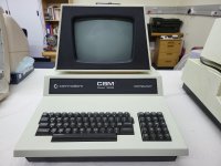
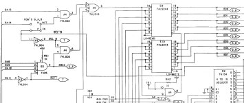
3032-01.jpg
1. With onboard ROM and RAM the machine won't boot, though the random display screen shows.
2. With all ROMs and IO chips out and with a RAM/ROM replacement board, mapped to BASIC 4 and 32KB of RAM, the machine boots to the BASIC 4 boot screen (but clearly no flashing cursor).

######################################
3. With all ROMs and IO chips out and with a RAM/ROM replacement board, mapped to BASIC 2 and 32KB of RAM, the machine boots to a blank screen.
4. With all ROMs out and with a RAM/ROM replacement board, mapped to BASIC 2 and 32KB of RAM - and with a 6522 installed, the machine boots to the BASIC 2 boot screen (but clearly no flashing cursor).
.
@daver2 , I specifically tested the above (2 & 3) to confirm what we saw in the recent 2001 repair, viz. with all ROMs in place, but no IO chips, BASIC 4 will boot to the BASIC screen but BASIC 2 will only show a blank screen. With a 6522 installed, BASIC 2 will then show the BASIC boot screen. I.e. a 6522 (but not the 6520s) are needed to get to the BASIC 2 startup screen. Just a point of interest.
######################################
.
Anyways, back to this machine and here is the bit of interest:
.
5. With a working Kernal and PETTESTER V4 I get the first PETTESTER screen. However, it never goes past this screen / test. Just stays here.
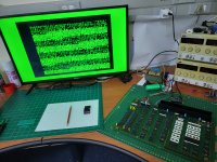
3032-04.jpg

My understanding is that this means PETTESTER is not passing the VDU test. However, I cannot, for the life of me figure out what is failing. The PETTESTER screen seems stable (no characters changing, etc.), I've confirmed the two 2114s are fine and when the machine boots into BASIC, I get a clean screen with just the expected BASIC boot screen.
.
I've also tested and replaced all 4116s that failed in my memory tester. But I also get the same with a RAM board mapping the RAM out, i.e. PETTESTER never goes past this first screen with either mapped out RAM or the onboard RAM.

Any ideas?
 
The PETTESTER can inevitably WRITE correctly to the video RAM but not READ back correctly from the video RAM.

As the display is correct (I assume it is) then the video RAM writing and reading is fine (otherwise the screen would not display correctly).

This smacks of a data bus buffer fault in the READ direction between the video RAM and the CPU.

Dave
Does feel like it. Going to start tracing that path.
.
But check this out......
To test the video and system RAM, I plugged a PET diagnostic board in, the one that puts a small microcontroller in the CPU socket. It writes and reads the video RAM fine (not sure how extensive the video RAM test is but is seems to be happy it's reading back what it wrote). It did give some errors on the main RAM, which I swapped.
.
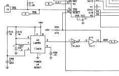
BUT.....while doing the main RAM test, the machine will reset randomly. I could see the reboot is caused by the Reset pin on pin-40 of the 6502 socket going low for about 500ms. Clearly the 555 is dodge, right?
.
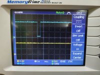
Except, it's not. Watching the output of the 555 shows it's stable when the pin-40 input goes low. The trace below is the input and output of hex buffer A10, specifically pins 13 and 12 which drives the reset signal on the CPU.Reset-01.jpg
Yellow is the input to the buffer on pin-13 and blue the output on 12.

Reset-02.jpg
Reset-03.jpg
You can see that the input (Yellow) to the buffer (as well as the output of the 555 and the inverter between them) are nice and stable when the output of the buffer (Blue) will go low for around 500ms. This period is pretty stable, as if the signal is intentionally generated.
.
My understanding is that the 555 is the only source for a reset signal on the board? The IO chips are out which are the only other places where the reset goes, if I read the diagram correctly. I did take the 7417 out and it tests fine in my chip tester but I'm not sure the chip tester would pick up something like this. (I need to go buy new buffers to replace and see if it resolves the problem.)
.
Seen something like this before?
.
Added: I replaced the 7417 with a 74LS07 but get the same results.
 
Last edited:
Interesting...

The other thing to check is CPU pin 7 (SYNC) is pulsing. This pin indicates that the CPU is fetching and executing instructions.

We have been in the situation before where PETTESTER has written the pattern into video RAM - and then the CPU goes off into the weeds and doesn't execute any more instructions - leaving the test pattern on the screen.

The 7417 is an open collector - so it would be wise to check the R30 pull-up resistor.

After that it would be advisable to follow the reset PCB track looking for short circuits or debris.

Dave
 
Well the 7417 or 74LS07 are open collector types that use a pullup resistor on the output. So if you see the signal there go low (assuming their inputs are not driven), it is something on their output pin pulling them low.

Since in the original configuration that /RESET line is connected to the CPU's reset pin, that is an input so that the CPU cannot be doing it, if there was an actual CPU in there.

But you said this:

To test the video and system RAM, I plugged a PET diagnostic board in, the one that puts a small microcontroller in the CPU socket.

This tends to suggest that the PET diagnostic board (whatever that is) is actively pulling the /RESET pin 40 line low. Since that low reset pulse you are seeing is perfectly rectangular, likely the pullup resistor is fine.

(in addition the 555 timer has a one second period, not 500mS, more evidence that it is not part of the problem)

I'm not sure what sort of fault finding pathway you are on, but it pays to minimize all variables and possibly adding a micro-controller is not the way to do this, unless say you were the one who programmed it and understands exactly what it is doing.

Generally most start with the NOP tester to help check out a lot of the hardware, then to Daver2's PETTESTER and after that to ROM/RAMulators. I use other methods myself but they don't lend themselves as well to explaining all the small steps to others.
 
Last edited:
On the magic-reset: The pull-resistor is in place. Fully agree that it looks suspiciously like the tester pulling the Reset line low as I've tested all the way from the 555 through the inverter to the buffer and it's only on the output of the buffer the I see this.
.
The tester actually measures the reset pulse and reports it, so it's (or rather should be) an input on the uController. I've used it a lot on 8032s but this is the first time on a Dynamic, non-CRTC, so could well have a bug.

I don't see the same random reset generated while PETTESTER is running but then it never gets to testing the main RAM.

My focus is first going to be to figure why PETTESTER stays stuck on the VDU test. Not at home now, but before I left, it did look like the 2 main databus buffers had no activity on their select lines, pins 1 and 19. The triple input NAND driving them (7410) had no activity though the 3 inputs were all wobbling.

Interestingly, with the uController in place, I do get the databus buffers being selected and the NAND driving them giving an output. Which seems to suggest the gate is working. My current working conspiracy theory is that it stops working when running at full speed, whereas (I suspect) the uController might be running at a much lower speed.

I'll be able to look at it again in an hour or two.
 
Your conspiracy theory may prove to be correct...

If the CPU 'misreads' an instruction somewhere it is 'curtains'.

CPU pin 7 will give you that information.

Dave
 
Your conspiracy theory may prove to be correct...

If the CPU 'misreads' an instruction somewhere it is 'curtains'.

CPU pin 7 will give you that information.

Dave
I'll double check but sure pin-7 stayed active while the PETTESR VDU screen is displayed, but I'll confirm.

I'm running a BASIC 2 Kernal and v4 from a RAM/ROM replacement board, I'll try a set plugged into the board as well to see if the test code hangs if running from ROM sockets.
 
Confirmed that CPU continue to run (i.e. pin-7 activity) with both a ROM set on the replacement board as well as with a Kernal + V4 plugged into the board.
.
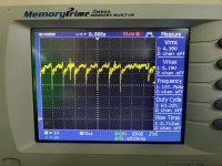
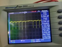
Below the output of the NAND gate (pin-6) driving the /G (pin-19) of the Data Bus buffers (E9 & E10). This clearly is not right, especially since the inputs of the gate are all looking good.
.
Question now is it the output of the 7410 or one of the 244 buffers pulling this high.
.
Think I'll socket the 7410 so I can test it, suspect it's going to pass. But it'll allow me to lift pin 6 so I can see if it comes alive. If it does, I'll have to pull the DBx buffers.


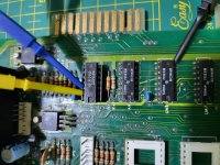
20230617_134137.jpg

BD Buffers.jpg
 
I will go for the gate being bust...

Dave
Think your money is safe. :)
.
I took it out and, as suspected, it tests fine in two different logic testers. Put it back in the board but lifted pin-6 out of the socket.
.
20230617_144232.jpg
.
Still get this as the output.
20230617_144207.jpg
.
Problem is, I don't have spare 7410s.... :(
 
I think the output, pin 6 of the 7410 is functionally high and it doesn't quite get to a logic low, and the low going transients probably represent a timing disparity of signals on its input changing state at nearly the same time, producing runt pulses at its output. Likely there is nothing wrong with the 7410. The inputs to the gate could "look right" checked one by one.

The designers have drawn the gate in its De Morgan equivalent suggesting its "active" state is for the output to be high when any input is low. Might be academic as it output gets inverted by A4 for R/W control, so it is active high for writes and low for reads. If say at some moment, considering the inputs if they are changing state where there is a timing skew between the buffered R/W signal from the CPU and the buffered address lines, small glitches like this could occur and the gate still be normal.

The thing is to check is the input pulse relative timing.

What does the output look like (or the input pulse's relative timing) with the normal CPU in position ? I'm thinking that running anything other than a 6502 CPU in the socket on its own (but I'm not sure what you are running) could result in an effect like this. Or maybe the there is a problem with the rising or falling edges of the buffered R/W line, pin 4 of A10.
 
Last edited:
Man, this thing has me running in circles. First order of business now is to break out a decent Merlot before I carry on.
.
@Hugo Holden , you might well be right that the 7410 is working, I found another one on some computer board from the 70's and scavenged that. It gives exactly the same output. I'm getting some new 74LS10s tomorrow, just as another test. The only way I'll be able to check if it is doing its thing correctly is to connect a logic analyser, which I've got - and can do - but, being lazy, I was hoping replacing it would do the trick.
.
I eventually decided to socket the 3 chips the 7410 is driving, being the 2 '244 buffers (E9, E10) and the 7400 (A4). Here's the kicker, one of the buffers were faulty (as tested in a chip tester) and when I desoldered A4, it came out with pin-1 missing in action. I suspect it was rusted off and fell off in the desoldering process. Socketing these 3 chips and installing new (tested) ones did not resolve the original problem (PETTESTER not passing the VDU test).
.
Clearly this machine's got multiple problems, faulty chips, corroded pins, etc. So I'm going to start from scratch and slowly work from 1st principles. For example, even with all the faulty 4116s replaced, the system will still only boot to BASIC with a RAM/ROM replacement board. So clearly more logic/buffering/decoding issues to find and resolve.
.
But first I need to attend to my moral duty to support the local wine farms, while watching the Canadian qualifying. And, tomorrow, morning, my RD350LC needs to go stretch her legs. Then it's back to the PETs. :)
 
There are two (2) more buffers for the video RAM at E7 and E8 as well...

Interestingly, buffers E9 and E10 drive the DRAM. There are also two (2) more data buffers here (I10 and I11) as well...

We were just debating about whether we were going to watch the Cricket and record the F1 qualifying or vice-versa...

Have a good evening. But remember, do not drive a PET (or an RD350LC come to think of it) under the influence of alcohol :)!

Dave
 
The only way I'll be able to check if it is doing its thing correctly is to connect a logic analyser, which I've got - and can do - but, being lazy, I was hoping replacing it would do the trick.

Possibly not to examine a timing skew problem.

Some logic analyzers artificially re-create the waves, so that the rising and falling edges that you see on the scope or screen display are generated by the analyzer itself and the output pulses look or appear perfectly rectangular and very small timing errors of the type that produce runt pulses with a logic gate can be very hard to spot.

The better move is to examine the input signal with a two or multi-channel scope, especially if it has a good delay time-base then you can expand an area out and inspect the relative timing of the waves as they rise & fall.

You said:

1. With onboard ROM and RAM the machine won't boot, though the random display screen shows.

I assume you mean the random screen that appears briefly at power up due to the 555 reset.

The usual cause for this is bad DRAM or bad DRAM control signals.

If this is the case I would go back to the beginning and start there. Fit the 6502 CPU no other custom hardware and fit known good tested & verified ROM's.

(are you 100% sure your DRAM IC's are ok and your 2114's too, you have testers for both types of IC ?)

Check the CPU is running.

Try the bank 4116 swap trick first, or don't fit the IC's to the upper bank to see if you can achieve a boot .
Inspect the over 20 pulses that control the DRAM on the scope that are in the article I posted.
(while you are there check the output of the 7410 again for those runt pulses they might be gone)
Try the NOP generator looking for problems in the hardware.
Try the PETTESTER again.
Move back to the ROM/RAM boards then if still no luck.

Just in case something got missed along the original testing pathway pathway.
 
Thanks for all the inputs @daver2 and @Hugo Holden, I'll respond to the various points you raised. Just want to give a quick update:
.
I started from scratch and checked all the obvious stuff, like voltages, clocks, reset, interrupts, etc. Then installed a NOP generator and check the address lines and relevant select signals. Those also looked good.
.
@Hugo Holden , I've already tested - and replaced - any faulty RAM, both 4116 and 2114.
.
I kept on being drawn back to that strange signal seen on the enable signal (pin-19) of the two main data bus buffers (E9 & E10). I've already established that the gate driving them, and the chips being driven by it, are fine.
.
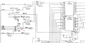
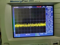
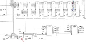
With PETTESTER running (and stuck on the VDU test), I started tracing backwards from A5 and found the output of pin-6 of B2 to be fixed at about 2V. All the inputs of that gate looks good.
.7425-08.jpg
.
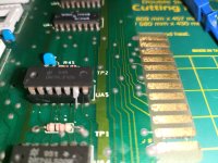
7425-01.jpg
.
B2 is a 7425 with two 4-input NOR gates. When I looked at the other gate, it gave exactly the same output, i.e. around 2V static, with inputs wobbling.
.
7425-10.jpg
.
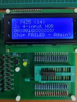
I've learned my lesson to blame TTL levels too quickly but this can't be right. So I decided to take it out and test it, and it fails a simple logic test.
.
7425-02.jpg
.
Been spending my Sunday going through a truckload of various cards/pcbs I've got in the store to see if I can find a chip to scavenge but no luck. I'll have to order and get back to this next weekend as I'm travelling for work this week. :(
 
Good work.

Well, we can't have every chip available...

No problem in having a break while we wait for the bits...

Dave
 
Thanks for all the inputs @daver2 and @Hugo Holden, I'll respond to the various points you raised. Just want to give a quick update:
.
I started from scratch and checked all the obvious stuff, like voltages, clocks, reset, interrupts, etc. Then installed a NOP generator and check the address lines and relevant select signals. Those also looked good.
.
@Hugo Holden , I've already tested - and replaced - any faulty RAM, both 4116 and 2114.
.
I kept on being drawn back to that strange signal seen on the enable signal (pin-19) of the two main data bus buffers (E9 & E10). I've already established that the gate driving them, and the chips being driven by it, are fine.
.
With PETTESTER running (and stuck on the VDU test), I started tracing backwards from A5 and found the output of pin-6 of B2 to be fixed at about 2V. All the inputs of that gate looks good.
.View attachment 1259192
.
View attachment 1259195
.
B2 is a 7425 with two 4-input NOR gates. When I looked at the other gate, it gave exactly the same output, i.e. around 2V static, with inputs wobbling.
.
View attachment 1259193
.
I've learned my lesson to blame TTL levels too quickly but this can't be right. So I decided to take it out and test it, and it fails a simple logic test.
.
View attachment 1259194
.
Been spending my Sunday going through a truckload of various cards/pcbs I've got in the store to see if I can find a chip to scavenge but no luck. I'll have to order and get back to this next weekend as I'm travelling for work this week. :(
There are three things here that are not quite right:

1) if both the gate outputs are looking defective with a borderline logic level, it would imply that both gates in the IC have failed in the same way, can happen but a lot less likely than one failing.

2) we have previously established on the Forum that at least one brand of IC tester is unable to test 7425's and reports them as defective when they are not. The designers of the tester ignored the additional pin on the 7425 (pins 3 and pin 11 that activate the gates). In this case I would not believe the tester until you had verified testing some other 7425's. It wouldn't surprise me if no tester out there could correctly test the 7425.

3) It is not a wonderful idea to keep removing chips for testing unless there is solid evidence that they have definitely failed. If this IC had failed it disables memory reads from the DRAM, so there would be no pulses at all on pin 8 of G7 IC and that would be stuck high, so that would be a good place to check with the scope to help confirm.
 
Last edited:
There are three things here that are not quite right:

1) if both the gate outputs are looking defective with a borderline logic level, it would imply that both gates in the IC have failed in the same way, can happen but a lot less likely than one failing.

2) we have previously established on the Forum that at least one brand of IC tester is unable to test 7425's and reports them as defective when they are not. The designers of the tester ignored the additional pin on the 7425 (pins 3 and pin 11 that activate the gates). In this case I would not believe the tester until you had verified testing some other 7425's. It wouldn't surprise me if no tester out there could correctly test the 7425.

3) It is not a wonderful idea to keep removing chips for testing unless there is solid evidence that they have definitely failed. If this IC had failed it disables memory reads from the DRAM, so there would be no pulses at all on pin 8 of G7 IC and that would be stuck high, so that would be a good place to check with the scope to help confirm.
1) Agree, it seems both gates failed. Definitely both give the same 2V level on their outputs while having valid signals on their inputs..
.
2) Yeah, I noticed only one of my two chip testers support the 7423 / 7425. The one that does, failed it. I'll get new ones this week, then we'll be able to test both the chip tester and the PET.
.
3)I'm with you on needlessly removing ICs. I desperately want to keep boards as original as possible and subscribe to the measure twice, desolder once philosophy. If I take a chip out and it turns out not to be faulty, I don't sleep well for a while. :)
 
Back
Top