• Please review our updated Terms and Rules here

3032 - 2001N Repair

Have not had a lot of time but here's where I'm at the moment:
.
After getting the intermittent issues around the IO chips (upper/lower case, flashing cursor coming and going/etc.), I replaced the four 4-pin white sockets with new double-leaf units. Fully expected the machine to just boot up and run reliably but now it would not boot at all. :oops: For example, PETTESTER now gives this screen......
20230624_01.jpg
PETTESTESTER clearly tried its best, but something is very wrong. (Got the same screen with the IO chips removed.)
.
Rechecked soldering and looked for signals on the chips themselves. This all looks good except A6 on the CPU (blue dot below) gave a very unhealthy signal. Looking at the signals around the relevant address buffer (C3 and B3) showed suspect activity on A5 and A6. A second CPU showed the same, so I plugged a NOP Generator to trace the address bus. All the signals looks perfect except AB5/BA5 and AB6/BA6.
.
20230624_02.jpg
.
AB5 (red dot) gives a healthy looking signal with a period of 128us as expected:
.
20230624_A5-CPU-pin-14.jpg
.
Looking at BA5 (yellow dot - pin-7 of C3), it looks like this. Remember its input is clean as per above (red):
20230624_A5-Buf-pin-7.jpg
Immediate suspicion would be that something is pulling the output of this buffer down, but somehow on every second pulse?.
.
AB6 on the CPU (blue dot), however, gives a very unhealthy signal. One would expect a square wave with a period of 256us but there seems to be a double pulse with the extra pulse at 1.8V:
20230624_A6-CPU-pin-15.jpg
.
BA6, the corresponding output of the buffer (green - pin-12) seems to "correct" these levels and give a square wave with a period of 128us, essentially what should be on A5 with a NOP generator:
20230624_A6-Buf-pin-12.jpg
.
I know the CPU is good, so it must be the buffer, right?
.
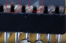
Did not have time to work on it further yesterday, and this morning woke up with a bit of an epiphany that there must be a short on the board causing this.
.
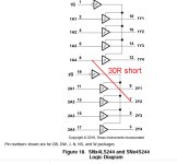
Looking at the circuit, I think it could easily be a short between pin-7 and pin-8. It would definitely explain why a 128us signal is appearing on A6:
20230624_02a.jpg

If it's electrical or mechanical I'll try and figure out later when I get back to the workshop. I tend to keep the working surface clean and did wash the board with flux remover and isoprop after replacing the four 40-pin DIPs but the fact that an "A5-like" signal is appearing on A6, and the relevant pins happen to be adjacent, seems highly suspicious.
 
Last edited:
One thing that can save you; If you are replacing IC's and fitting sockets, which is often the case, it is required to carefully study the pcb under very high magnification, before the new sockets are fitted, because the plastic body of the socket obscures the view once it is fitted. Often there is a temptation to rush a repair, but if something is missed in this sort of area, it can cause a major headache later.
 
Some updates:
.
Measured for a short between pin-7 and pin-8 of the 244 buffer and it measured ~30 ohms! Other, similar pins, measured 10s of Mega ohms.
.
Looking for a mechanical short both on the bottom and top side of the board did not show any obvious shorts:
244-10.jpg
.
So took out the buffer and measured it out of circuit:
244-12.jpg
.
And saw the same ~30 ohms between pins 7 and 8:
244-14.jpg
.
It also failed in 2 different chip testers:
244-18.jpg
244-20.jpg
.
Put a new 244 in and we're back in business:
244-30.jpg
.
Hopefully I can now get to testing the IO ports, including the cassette and IEEE ports. (I did strip and clean the keyboard and it went from mostly non-functional to working perfectly.)
.
It does make you wonder what else will fail along the way. But that comes with the territory, I guess.
 
Last edited:
Nice diagnostic skills...

It shows the advantage of using the right diagnostic tool for the job and following a logical diagnostic process.

Eventually, either you will beat the PET into submission - or it will kill you!

Dave
 
Nice diagnostic skills...

It shows the advantage of using the right diagnostic tool for the job and following a logical diagnostic process.

Eventually, either you will beat the PET into submission - or it will kill you!

Dave
Oh, 100%. The only winner here is the local vineyard...... 🍷🍷
 
Wow, that is an unusual IC failure to get a low R short between those two pins since they are not near the same gate structure in the IC die, though they may be close on the actual die perimeter. One thing that links them together is the proximity on the IC package too, which would have made it seem much more likely that the short was external to the IC body. It is hard to imagine how that came about inside the IC. That is one for the books. Also the 244 is generally a fairly reliable part too.

Looking closely at your photo there appears to be a white deposit on the IC body between pin 7 & 8, I wonder if that is conductive ? Or was it a brown deposit initially and you scratched between the pins ? There is also a brown deposit, possibly rust, from the pins, between pin 5 & 6.
 

Attachments

  • LS.jpg
    LS.jpg
    93.2 KB · Views: 6
  • LS2.jpg
    LS2.jpg
    244.5 KB · Views: 5
Last edited:
Wow, that is an unusual IC failure to get a low R short between those two pins since they are not near the same gate structure in the IC die, though they may be close on the actual die perimeter. One thing that links them together is the proximity on the IC package too, which would have made it seem much more likely that the short was external to the IC body. It is hard to imagine how that came about inside the IC. That is one for the books. Also the 244 is generally a fairly reliable part too.
Looking closely at your photo there appears to be a white deposit on the IC body between pin 7 & 8, I wonder if that is conductive ? Or was it a brown deposit initially and you scratched between the pins ? There is also a brown deposit, possibly rust, from the pins, between pin 5 & 6.
Absolutely made much more sense that it would be a mechanical short between adjacent pins. I also saw a patch of oxidation between pins 7 and 8 on the body of the chip that I cleaned before unsoldering the 244. I did not take a photo of it but saw it under the microscope. Cleaning it did not resolve the short. As you saw, when I took the 244 out, the short stayed between the two pins. Fully agree this is one for the books. Where an output of one gate developed a short to the input of another. Must be something with the internal construction of the die and chip itself.
.
These chips are all badly corroded, and I wonder what else might be brewing.
 
Last edited:
There is also a phenomenon called 'tin whiskers' that I have seen before.

Microscopic growths of tin that can form whiskers between adjacent pins etc.

The purer the tin, the more easily they form. Particularly relevant for lead-free solders containing more tin, but also seen in leaded solder on old equipment.

Dave
 
To keep track, so far I've unsoldered 616 pins on this board.
.
These include:
.
- 16 x 4116 DRAMs, of which 15 were faulty
- 2 x 2114 VDU RAM, both which were fine
- 5 x 74244 buffers, of which 2 were faulty
- 3 x glue logic, of which, at least, 2 were faulty
- 4 x 40-pins sockets, because they were white
.
The fact that I could unsolder these chips, socket them and carry on, is a massive nod to the PET PCB quality. In unsoldering all these, not once did I see a pad or track that looked slightly damaged or in distress. If this was a TRS80 Model 1, just looking at the tracks would made them lift........
.
With so many chips socketed, this might just become my test board for future repairs, especially when testing 6502, 6522 and 6520s. I'm seriously considering socketing the ROM sockets as well. In for a penny, in for a pound, as they say......
 
There is also a phenomenon called 'tin whiskers' that I have seen before.

Microscopic growths of tin that can form whiskers between adjacent pins etc.

Dave
Exactly why I pulled out the high-def microscope. Definitely did not see them on the solder side, but you never know what lurks under the chip. (I did try and clean under the chip, while it was soldered in.)
.
In this case, with the chip out the board, it was still there.
 
Certain people see a PET with white sockets and immediately warm up the soldering iron...

Dave
Indeed, I was quite torn in replacing these. Definitely had both positive and negative experiences with them. In some of my 8032s, I have to fiddle with them, every time I (attempt to) boot the machines. In other cases, and especially if you fit new chips, they seem OK. My reading on this is that your best bet would be; new chips, with unoxidised pins, at an outwards angle, that can go down deep into the white sockets.
.
But, definitely not where you are fiddling a lot, especially with original chips. With this board, there were just too many variables being thrown up and, eventually, I decided to replace them. Up to this point I was hoping to protect them by plugging a modern double-leaf socket into them and plugging chips into those.
.
BTW, I tried the @Hugo Holden trick of pushing a pin into the white sockets and test the insertion resistance, and was (not so pleasantly) surprised by the lack of any such resistance.
 
Spoke with Stephan and he confirmed the 7425 passes in his own RCT tester. I'll do some debugging on my side, probably fluffed something........
I read your message and I have also tested a 7425 with RTC (Latest public firmware) and this one is failing for me also. Tested with 3 new 7425 IC's.
 
I read your message and I have also tested a 7425 with RTC (Latest public firmware) and this one is failing for me also. Tested with 3 new 7425 IC's.
Here's the problem I found. See screenshots below.

@Hugo Holden would also be interested in this;
.
When testing the logic functions of the chip, it all works (level wise) and the gates are tested properly.
.
However, when the gate (pin 3 / 11) is pulled low, it drives the output NOT HIGH enough to register as a high. And thus the test seems to fail.
.
I've given Stephan this info. It passes in his tester and is likely a function of components in the test device itself. I'll try and change the Zener diodes and see if it helps.

7425-pin-1.jpg
7425-pin-2.jpg
7425-pin-3.jpg
7425-pin-4.jpg
7425-pin-5.jpg
7425-pin-6.jpg
7425-VCC.jpg
.
This is the key output; You can see the output not going high enough (the second pulse) when the Gate input goes low. This is the problem with the chip seemingly failing in the RCT.
7425-pin-6.jpg
 
In most applications for the 7425, the strobe input is tied high with a 1k resistor. Seldom have I seen any designers use it to inject a signal. It is actually quite useful in the case of the PET because pulling it low can inhibit memory reads. I used this feature in my DRAM diagnostic system where I inhibit the reads of the lower 2k of memory and dynamically switch in an SRAM.

Inside the chip this strobe input is connected to the additional emitters of the 4 input transistors on each gate.They are dual-emitter input transistors. To pull it properly to logic low, will take the same amount of low drive (current sinking) as 4 TTL gate inputs, and these for plain 74 series devices are higher than 74LS devices. The data sheet says 6.4 mA to get a 0.4V low, which, if you had a pull down resistor would be 62 Ohms.
( versus say just a single 74 series input would be around 250 Ohms) For LS TTL the input currents for a logic low are only 1/4 of that and for a single gate input a 1k works to pull the input down to 0.4v.

When the 7425 strobe input is pulled successfully logic low, the gate behaves as though all of its inputs are logic low (even though they might not be) so the output of the gate should be stuck high and the gate unresponsive to any/all inputs.

Guessing here: Probably the tester would test a 74LS25 ok but not the plain 74 (maybe Stephan was testing LS explaining why his tester works and yours doesn't?), possibly due to a limitation in the hardware not expecting to have to sink 6.4mA or so, on the strobe pin on the 7425.

These sorts of differences are the reason why, say if you are replacing the chips in vintage computers, it pays to stick to the exact type, plain 74, LS, S, H,L etc. Often people grab a similar part like 74HCT which would appear ok, etc, but the thing is you never can be 100% sure that is ok, it mostly can be, especially substituting in LS for plain 74 , but there can be odd input and output level anomalies and timing ones too, so it is always better to use the exact part.
 
Last edited:
Quick update on this machine:

1. Keyboard cleaned and working well.
2. Cassette ports tested and working.
3. IEEE port tested and working.
.
A short note (and gotcha) on the IEEE port test program from the book below. This is a really handy program and has helped me a lot in the past to find faulty components in the IEEE circuit.
.
When running BASIC 2, the program will return a "ATN IS BAD" message, but will not do so with BASIC 4. This is with a known working set of components. Also, a drive works fine on the port. So some different routines in the two BASIC version.
.
.
20230701_131753.jpg
.
This caught me out with a 2001 before, running BASIC 2. When it threw up the 'ATN' error, I went and replaced the corresponding bus driver only to find out it was fine.
.
Cover.jpgIEEE Test.jpg
.
PS. If someone wants the BASIC listing, I can post it. Typed it in, from the book a long time ago.
 
Started on the 9" monitor of this 3032. It turns on but gives a very out of proportion vertical size. From this screenshot, you can see how much the text is stretched.
.
Vertical size - 02.jpgVertical size - 01.jpg
.
Adjusted the vertical size trim-pot (R20, 1Mohm) but it made no difference. Tested the pot in-circuit and it read about 200K and with no (or very little) change in resistance when adjusted. Took the pot out and one leg fell off when it came out, so clearly broken.
.
Did not have a direct trim-pot replacement but found a 1M5 lin pot that I wired in. But got exactly the same result, the vertical size is significantly stretched, and the vert size adjustment makes no difference.
.
This is where I stopped for now. Must now first figure out how to easily test and work on this board before proceeding. Any tips on how you guys work on these monitors (where the board is essentially inside the case due to short cables) or any ideas on how to rig a jig of some sort will be appreciated. ( @Hugo Holden, I did read your excellent paper).
.
In terms of the vertical size being over-stretched and the trim pot making no difference, any initial thoughts would be appreciated. I will start measuring down the vertical-drive path as soon as I figure out how to get to the bottom of the board while still connected to the tube. But hoping this is a known symptom with a known cause. :)
 
Back
Top