• Please review our updated Terms and Rules here

AUVA JUKO Baby XT BXM-10

I grounded the isa slot pin 10 - with rudds rom still in - speaker sounding - the address line reads 3.8 to 4V for high and 0.13V for low,
i get the result exactly as the procedure describes FFFF0 !
1663629910370.png
Also, it doesnt appear pin P8-1 (power good) connects to anything on the motherboard. Holding it up to the sun I can’t see any traces from this pin. And sounding out nearby test points there is nothing connected to pin p8-1. where should pwr good go to ? Is it possible the board is designed for a psu where the 5v rail is used as power good ?
 
Last edited:
I have the parallel post code reader.
With standard phoenix bios it gives “00 FF”. It really doesn’t seem to get anywhere after I flick on the power.
Do not expect the 2.52d BIOS to output diagnostic codes to parallel ports.

We use Rudds Diagnostic ROM because we do now that it does output diagnostic codes to parallel ports, and we know what those codes mean.

with Rudds Diagnostic rom, i get a short beep, ...
That is a good sign. At [here], you can see that Rudd's diagnostic ROM beeps the speaker at step 25. But a question is, is it the same beep ?

with Rudds Diagnostic rom, i get a short beep, then several things flash on the post code reader before it hangs :
the sequence reads :
So: 04, 00, FF, 00, 01, 02, 03, 04, 7E.

The '00, 01, 02, 03, 04, 7E' is what we are interested in. It suggests that, per [here], the reader is seeing checkpoints 00, 01, 02, 03, 04, then something bad happens.

Is that repeatable, i.e. do you always see 00, 01, 02, 03, 04, 7E ?
 
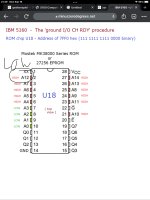
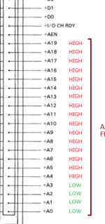
Continuing the grounded pin 10 proceedure, when i check the lines at the bios chip A12 is low when it should be high. All the other address lines read as in the figure. 302598E2-7F88-4005-A007-0662B9D09241.jpeg
 
Is that repeatable, i.e. do you always see 00, 01, 02, 03, 04, 7E ?

Yes, unless I do something like switch the power on-off-on - this gives me some very random results, including 3 different tones from the speaker on different occasions.

Also if I change the 2 video related switch block switches on the mainboard we get other final codes i.e 7E 82 …
 
Continuing the grounded pin 10 proceedure, when i check the lines at the bios chip A12 is low when it should be high. All the other address lines read as in the figure.
That is a problem. The A12 pin (pin 2 on a 28C64) is expected to be a logic high during the 'Ground IO CH RDY' procedure.

Using a multimeter on my very-similar-to-yours motherboard, I observe that the A12 signal for that pin is connected to a pin on the flatpack chip, and connected to pin 7 (an input pin) on the middle of the three 74LS373 chips. Is your motherboard the same?
 
Last edited:
Yes, unless I do something like switch the power on-off-on - this gives me some very random results, including 3 different tones from the speaker on different occasions.

Also if I change the 2 video related switch block switches on the mainboard we get other final codes i.e 7E 82 …
Inconsistency.

There certainly appears to be inconsistency with the A12 line: When you earlier saw 00, 01, 02, 03, 04, 7E from Ruud's diagnostic ROM, the A12 line to the 28C64 must have been HIGH at the time that the CPU came out of reset (i.e. CPU started execution from motherboard address FFFF0 hex, which is address 1FF0 hex {1111111110000} within the 8 KB sized BIOS ROM )

Put the 8 KB sized code at [here] into a 28C64 and see how that goes. All that the code does is send the 4 bytes of {00}{FF}{55}{AA}, in that order, to LPT ports 378h, 278h, and 3BCh, then it halts the CPU. So, the last 4 codes seen on your parallel port code reader should be {00}{FF}{55}{AA}, in that order. You may be interested to see if you get consistent results running that.

(There is a small delay between the 4 bytes, otherwise, as I discovered, the parallel port code reader misses bytes.)
 
That is a problem. The A12 pin (pin 2 on a 28C64) is expected to be a logic high during the 'Ground IO CH RDY' procedure.

Using a multimeter on my very-similar-to-yours motherboard, I observe that the A12 signal for that pin is connected to a pin on the flatpack chip, and connected to pin 7 (an input pin) on the middle of the three 74LS373 chips. Is your motherboard the same?
I get a connection between A12 on the ISA and 74LS373 pin 6 (U14 on the silkscreen), pin 6 is high when A12 is high.
I think pin 6 is the output from the 74LS373 based on the input at pin 7 ?

but I get no connection A12 to the flatpack chip (U1).
however, pin 7 the 74LS373 is connected to the Flatpack chip .
So far nothing connects to A12 on the bios !
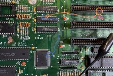
DA48984A-9CE2-43C6-B02A-AEEF1A288CF5.jpeg
 
Last edited:
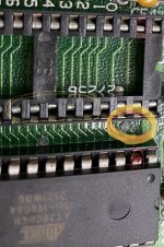
Found a problem- this via (thick circle) connects to the flatpack chip and 74LS373-pin-7, but it doesnt connect to the rom sockets A12 right next to it. It looks like the traces are corroded on both sides of the via, also blue corrosion in the 27256 socket. So should I put a bodge wire on the backside of the board?
I’ll run the 500.bin, 11111111…, 0000000.., 010101… , 101010… pattern bios before and after the fix just to make sure.

3FBEC85E-4F57-49A3-B196-A0D4C1814313.jpeg
 
Last edited:
I get a connection between A12 on the ISA and 74LS373 pin 6 (U14 on the silkscreen), pin 6 is high when A12 is high.
Your motherboard matches mine (except for the maximum motherboard RAM that can be fitted).

The A12 signal leaves the flatpack chip, going to:
- Pin 2 on both of the ROM sockets (U10 and U11).
- Pin 7 (an input) on the middle 74LS374 (with pin 6 driving the A12 signal onto the A12 pin of the ISA slots).

I think pin 6 is the output from the 74LS373 based on the input at pin 7 ?
Yes.

Found a problem ...
In a way, it is good that it is a socket problem. Had it been the flatpack chip, you may have had to throw the board away.

So should I put a bodge wire on the backside of the board?
You can try that. Per [here], I use them to bypass damaged vias. But you may end up having to replace the socket.

The pin 22 contact in the U11 socket looks problematic:

1663727154271.png
 
So, the last 4 codes seen on your parallel port code reader should be {00}{FF}{55}{AA}, in that order.

with the 500.bin bios and a broken A12 line the Parallel port reader stores :
position 01 = {00} 0000 0000
position 02 = {FF} 1111 1111
position 03 = {00} 0000 0000
position 04 = {FF} 1111 1111
position 05 = {55} 0101 0101
 
Last edited:
with the 500.bin bios and a broken A12 line the Parallel port reader stores :
position 01 = {00} 0000 0000
position 02 = {FF} 1111 1111
position 03 = {00} 0000 0000
position 04 = {FF} 1111 1111
position 05 = {55} 0101 0101
i put the bodge wire in place, now A12 is connected,
the 500.bin rom generates a continuous loop of 00 FF 55 AA....
now to try Ruuds Rom..
 
Oh dear, still not fixed then. Something is causing a crash and a reset?
With Ruuds rom in now I get a a nice normal startup beep!, then a continuous loop, where it displays 26 28 and 2A 2E on the parallel post card.
Also I tried hooking up my 5151 mono monitor to a 7 VEGA graphics card, the graphics card + monitor pair works in my 5160. I dont get any video.
View attachment D5315E01-3CC7-46FA-A279-CE30E8587991.MOV
 
So does 2A 2E mean that we are getting all the way to checking the first 2kb of RAM ?
Not necessarily. If there are addressing issues, who knows which parts are being executed and which are not.
To gain confidence, you would need to go through the previously received codes, expecting to see the sequence that is shown at [here], i.e. {00}{01}{02}{03}{04} ... {2A}{2E}

If TEST5055 and TEST5000 and TEST5077 do not display as expected, I see no point in trying Rudd's Diagnostic ROM.

You could still have IC socket problems (on different pins). I will look at my motherboard, and return here with a list a continuity checks you can do.
 
Is this socket compatible with 27C256?
You should see activity on all data lines.
You should see the chip select line toggling.
You should be able to verify that all address lines CAN toggle. If at steady state you can't see any one address line toggling, then try power cycling to see if you get a burst of toggles. If an address line = +5V, 0V, or has a distorted shape - look at the bus driver chip.
On the data lines, this is more tricky because they are bi-directional. I would look for clean edges and well formed data pulses; if there is an abnormal distortion that might indicate a problem. By abnormal I mean - different than the other 7 data lines.

If I am following the thread, is there an issue with A12?

If you can get a scope on A12 that would be good just to confirm you have a good logic signal. Wouldn't hurt to check others.

I'm guessing that this pcb uses internal layers to route address and data. That corroded via may be indicative of more corrosion under the socket, and possibly internal layer damage.


Verifying your address bus is good seems like a good thing to do. DVM probing may not be sufficient.
 
Last edited:
You could still have IC socket problems (on different pins). I will look at my motherboard, and return here with a list a continuity checks you can do.
ROM SOCKET U10

Pin 1 (VPP) has continuity to +5V line.
Pin 2 (A12) has continuity to pin 2 of '27256' socket (U11), and pin 7 of U14.
Pin 3 (A7 ) has continuity to pin 3 of '27256' socket (U11), and pin 8 of U14.
Pin 4 (A6 ) has continuity to pin 4 of '27256' socket (U11), and pin 13 of U14.
Pin 5 (A5 ) has continuity to pin 5 of '27256' socket (U11), and pin 7 of U13.
Pin 6 (A4 ) has continuity to pin 6 of '27256' socket (U11), and pin 8 of U13.
Pin 7 (A3 ) has continuity to pin 7 of '27256' socket (U11), and pin 6 of U15.
Pin 8 (A2 ) has continuity to pin 8 of '27256' socket (U11), and pin 13 of U15.
Pin 9 (A1 ) has continuity to pin 9 of '27256' socket (U11), and pin 8 of U15.
Pin 10 (A0 ) has continuity to pin 10 of '27256' socket (U11), and pin 11 of U15.
Pin 11 (D0 ) has continuity to pin 11 of '27256' socket (U11), and pin 9 of U12 (near V20).
Pin 12 (D1 ) has continuity to pin 12 of '27256' socket (U11), and pin 8 of U12 (near V20).
Pin 13 (D2 ) has continuity to pin 13 of '27256' socket (U11), and pin 7 of U12 (near V20).
Pin 14 (GND) has continuity to ground.

Pin 15 (D3 ) has continuity to pin 15 of '27256' socket (U11), and pin 6 of U12 (near V20).
Pin 16 (D4 ) has continuity to pin 16 of '27256' socket (U11), and pin 5 of U12 (near V20).
Pin 17 (D5 ) has continuity to pin 17 of '27256' socket (U11), and pin 4 of U12 (near V20).
Pin 18 (D6 ) has continuity to pin 18 of '27256' socket (U11), and pin 3 of U12 (near V20).
Pin 19 (D7 ) has continuity to pin 19 of '27256' socket (U11), and pin 2 of U12 (near V20).
Pin 20 (/CE} has continuity to pin ??? on flatpack chip.
Pin 21 (A10) has continuity to pin 21 of '27256' socket (U11), and pin 18 of U14.
Pin 22 (/OE) has continuity to pin 22 of '27256' socket (U11), and pin ??? of flatpack chip.
Pin 23 (A11) has continuity to pin 23 of '27256' socket (U11), and pin 17 of U14.
Pin 24 (A9 ) has continuity to pin 24 of '27256' socket (U11), and pin 13 of U13.
Pin 25 (A8 ) has continuity to pin 25 of '27256' socket (U11), and pin 14 of U14.
Pin 26 (not connected) has continuity to NOTHING.
Pin 27 (/PGM) has continuity to +5V line.
Pin 28 (VCC) has continuity to +5V line.
 
If I am following the thread, is there an issue with A12?

If you can get a scope on A12 that would be good just to confirm you have a good logic signal. Wouldn't hurt to check others.

I'm guessing that this pcb uses internal layers to route address and data. That corroded via may be indicative of more corrosion under the socket, and possibly internal layer damage.


Verifying your address bus is good seems like a good thing to do. DVM probing may not be sufficient.
A12 seems good now that I put a connection from the via to the pin. I measued High on it. We have 2 rom sockets U10 = 2764, U11=27256.
So far I only fixed the A12 connection to socket U10. A12 is also missing on U11. Seems like corrosion on both sides of the via. Now Im afraid that what I did not check was if the A12 line goes anywhere after U11. ..

The pcb seems to be only 2 layers ?so far I’ve been able to trace all the lines at the surface.

Both sockets probably need replacement, but I would be using a solder sucker and braid to get them off, so 45 mins or so. I plan to do this when I pretty up my bodge wire work.

I’ve still got my oscilloscope, so probing arround seems like the next step.
 
Back
Top