• Please review our updated Terms and Rules here

Can someone help me date my 5150?

I repaired it, I think it was pin 7 from the back on J4, which I think is IRQ4 for slot 4.
So if right I guess unless I plugged a card in set to IRQ 4, I'd likely never have noticed.
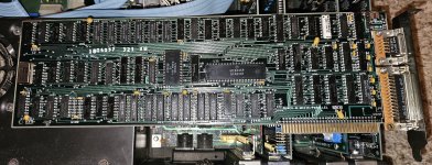
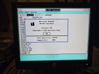
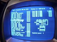
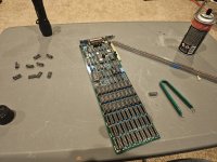
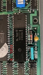
I brought out one of my 16KB-64KB motherboards, and 'lo and behold', I see:

1712294462042.png

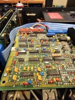
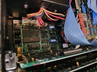
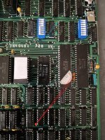
The affected via goes to pin B8 on the ISA connector. B8 is 'reserved' in the IBM 5150, and later, used for CARDSELECTED (slot 8 related) in the IBM 5160.

So, where was the trace heading off to? The motherboard circuit diagram in the first edition of the technical reference reveals what is going on.
It appears that:
- Initially, B8 was intended to be used for a 'HRQ I/O CH' signal, a signal that heads off to U52.
- Then, IBM changed their mind.
- In the first technical reference: Figure 3 indicates B8 as 'RESERVED', but the circuit diagram shows otherwise.

So maybe, on initial 16KB-64KB motherboards, the trace is intact. Later, IBM decide to disconnect the trace. Until new PCB's were produced that had the trace broken, a rotary tool was used to sever the trace.
 
So it works again, this time it was bank 1 chip 1 on the motherboard, after replacing it I added in one of the expansion cards and set the motherboard DIPs to 320KB but it looks like more ram is bad on the IBM 256KB card.
I've been reading your RAM listings, and I think it looks like I can replace the ram in the banks with 9 KM4164B-15 chips, does that sound right?
I get a 509C 201 error, but I can't seem to make it go away. I have swapped in other 4164 chips in to bank 0, and moved the old bank 0 into bank 1 (all 18 chips) and the 509C still stays. (the HMS told me it was bank 0 chip 3).
My math from your memory ram error image says it occurred in the 80th 4 KB block, with errors in bits 3 and 4, so right at the end of 320?
Can those 3 legged caps go bad on the IBM 64-256KB expansion cards and look like RAM chips? Or will the KM4164B-15 not work in the expansion card?
I even tried setting the Jameco to start at 64KB and use 256KB and it throws a 5055 error, same place, the end of 320?
Any ideas where to go next?
 

Attachments

  • IBM 64-256KB Memory Expansion Option.jpg
    IBM 64-256KB Memory Expansion Option.jpg
    3.1 MB · Views: 2
Last edited:
With the help from here and all your reference documents on www.minuszerodegrees.net I've gotten it back up (while waiting for the Rudd's to arrive in the mail).
I have the ST225 and WD12 both working (someone had set the primary ST225 to something way off). I had to set the controller and initialize it, then partition it and format it new.
I have Installed PC-DOS 3.3 and Windows 2.03 and it will boot from the ST225.
As soon as I started using your RAM sheet and not the MAP I realize the errors were at the end of each card and therefore the last banks, that let me move some RAM around and completely fix the IBM 256KB card, and then get at least 224KB of RAM working on the Jameco card. I still have to set the MB to 544 to get it to work (ignoring the last 32KB of the Jameco cards installed 256KB.
Thank you for helping me get this far, I can tell you without your site there would be a lot less success stories of people bringing the old IBMs back to life.
 

Attachments

  • 20240406_111313.jpg
    20240406_111313.jpg
    1.7 MB · Views: 4
  • 20240406_112752.jpg
    20240406_112752.jpg
    3.7 MB · Views: 4
With the help from here and all your reference documents on www.minuszerodegrees.net I've gotten it back up (while waiting for the Rudd's to arrive in the mail).
Good.

... and the 509C still stays. (the HMS told me it was bank 0 chip 3).
Some of the IBM documents need to be considered as a guide, not a bible. For example, the page of the HMS that you show in post #16 assumes a computer that was working one day, and then, one RAM chip failed.

There are other issues such as the motherboard switch settings in the first release of IBM 5150 documents, no longer applying because the motherboard BIOS was later upgraded to the 10/27/82 one.

I still have to set the MB to 544 to get it to work (ignoring the last 32KB of the Jameco cards installed 256KB.
Ruud's Diagnostic ROM has yet to arrive, but since you have the ability to run BASIC, you could try the BASIC code at [here], to verify that the motherboard switches are being read correctly.
It would be good to knock that check out of the way before investigating other things.
 
So I replaced all the failed RAM in the cards and onboard and I ran Rudd's Diagnostic, and it looks like there is something really wrong with either the dip switches for SW2 or whatever chip is being programmed by them.
After a bunch of tests, here is the complete output of all Dip switch settings.
00000 = 00000
00001 = 00001
00010 = 00010
00011 = 00011
00100 = 00000
00101 = 00001
00110 = 00010
00111 = 00011
01000 = 00000
01001 = 00001
01010 = 00010
01011 = 00011
01100 = 00000
01101 = 00001
01110 = 00010
01111 = 00011
10000 = 10000
10001 = 10001
10010 = 10010
10011 = 10011
10100 = 10000
10101 = 10001
10110 = 10010
10111 = 10011
11000 = 10000
11001 = 11001
11010 = 10010
11011 = 11011
11100 = 10000
11101 = 11001
11110 = 10010
11111 = 11011 (a couple of times 11111)
It looks like something is wrong with 2 and 3, but it interacts in a weird way with other switches.
It's why when I set 640KB of ram with 10110 I get a A055 error, because it doesn't set it for 640KB, it sets it for some weird undocumented 768KB state at 10010 and so the RAM above 640KB fails.
Has anyone seen this before? Where do I start to fix this? Is it just the dip? It seems like it is something that is using the DIP, not the dip itself.
I can set it to 544KB because of the 2 and 3 being at 00, but anything else is hit and miss, sometimes 2 and 3 will both register 11, but most times not.
I also attach a picture of it running the switch test in basic, same weird results.
What should I do next?
 

Attachments

  • 20240412_134143.jpg
    20240412_134143.jpg
    5.4 MB · Views: 9
  • 20240412_134136.jpg
    20240412_134136.jpg
    4.1 MB · Views: 9
  • 10110.jpg
    10110.jpg
    2.4 MB · Views: 9
  • 20240412_083736.jpg
    20240412_083736.jpg
    4.6 MB · Views: 6
  • 20240412_092806.jpg
    20240412_092806.jpg
    1.2 MB · Views: 6
  • 20240412_093531.jpg
    20240412_093531.jpg
    1.4 MB · Views: 7
Last edited:
What should I do next?
The switch block SW2 circuitry is shown below, restricted to the first 4 switches. Software commands the 8255A to take its PB2 pin to HIGH, then the software reads the first 4 bits of the 8255A's port C (i.e. PC0, PC1, PC2, PC3).

The PB2 output of the 8255A chip, and U63, are common to switches 1 through 4. Switch 1 is being read as expected (at 0 and 1). Therefore, we rule out the PB2 output of the 8255A chip, and rule out U63.

That leaves the switch block itself, resistor network RN2, the 8255A chip, PCB traces, PCB solder joints, and other bits of the PCB.

Let's pick switch 3. It always reads as off, apart from the "(a couple of times 11111)". Using a multimeter, measure the resistance of switch 3. In the ON position, its resistance is expected to be zero ohms, or say, 0.1 ohms. When then flicked to OFF, the resistance is expected to jump to much higher reading.

Assuming that switch 3 measured as expected, I would then ground pin 8 of U63, then measure the voltage on the PC2 pin of the 8255A chip:
Switch 3 OFF: PC2 pin expected to be about +5V ('pulled' to +5V via RN2).
Switch 3 ON: PC2 pin expected to be a TTL LOW output (0 to 0.5V).

If those two voltages are as expected, then it means that the 8255A must be faulty.
(I.e. With U63-8 at LOW, and switch 3 in the ON position, pin PC2 is LOW as expected, but the 8255A is reporting a HIGH instead.)

1713004613687.png
 
I've been trying to take measurements across the various elements, but I'm not used to doing this level of repair.
I can find schematics for the B255A so I can tell which pins are which, but I'm having to make assumptions for the pinout of the RN2 and when I test (what I think is pin 9 showing 2K instead of 8K referenced to what I'm assuming is pin 8 (5v?) of the RN2 I think it's the resistor bank that is faulty, but that's too many assumptions me me to start ordering parts (if I could even find a source for what I think RN2 is called, 316A822?)
Can you confirm that the test points I'm using are correct?
I get 8K from pin 8 on the RN2 to pins 9, 14, 15, but only 2K on pin 9 at anytime. (with the switches in the off position)
I never get any connection between U63 pin 8 and U36 pins 14, 15, 16, 17, they always show open even when 1-4 of SW2 is set to on. (which makes me think I doing it wrong).
 

Attachments

  • area.jpg
    area.jpg
    3.8 MB · Views: 4
  • B255A.jpg
    B255A.jpg
    1.5 MB · Views: 2
  • RN2.jpg
    RN2.jpg
    712.5 KB · Views: 4
  • U63.jpg
    U63.jpg
    2 MB · Views: 2
I think it's the resistor bank that is faulty
Note that those resistor networks ('RN') are very reliable.

You are making resistance measurements in-circuit. Depending on the circumstances, that is problematic. See [here] for an example. But you must be aware of that because you wrote "(with the switches in the off position)". Even with switches 1 through 4 in the OFF position, a question becomes, is the 8255 chip affecting the measurement of the four associated resistors in RN2.

The way that RN2 is drawn in the circuit diagram suggests a resistor network chip that is configured like [here], isolated resistors. And the PCB ties one end of each resistor to +5V.

Let me bring out a 16KB-64KB motherboard, and take a look, and confirm things, such as pin numbering. IBM is known to have errors in the circuit diagrams.
 
Let me bring out a 16KB-64KB motherboard, and take a look, and confirm things, such as pin numbering. IBM is known to have errors in the circuit diagrams.
I brought out a 16KB-64KB motherboard.

I concluded that RN2 contains 15 resistors, each resistor of 8K ohms, in a bussed arrangement per the image below. The PCB ties pin 16 to the +5V rail.

Here is what I measure:
1. Turn off all switches in both SW1 and SW2.
2. With digital multimeter in resistance mode, put black (repeat: black) probe onto pin 16 of RN2.
3. Put red probe onto pin 1. I measure about 8K ohms.
4. Repeat step 3 for pins 2 through 15, each time, I measure about 8K ohms.

You mentioned 2K ohms. I saw that too in certain situations. The problem of in-circuit measurements. Here is an example: RED probe (not black) onto pin 16 of RN2, and black probe onto pin 4. About 2K ohms is measured. Reverse the probes, and the measurement jumps to 8K ohms.

Some inter-resistor measurements are affected. Looking at the diagram below, expected between pins 1 and 4 is about 16K ohms (two 8K ohm resistors in series). I measure about 16K ohms if I have the black probe on pin 1, but I see about 15K ohms instead if the red probe is on pin 1.

I also confirmed that:
* SW2-1 is connected to pin 9 of RN2.
* SW2-2 is connected to pin 14 of RN2.
* SW2-3 is connected to pin 15 of RN2.
* SW2-4 is connected to pin 10 of RN2.


1713158121112.png
 
Last edited:
The RN2 diagram was invaluable, I had the pins completely wrong during my tests, and the probe color note was spot on, after switching the polarity around (and testing the correct pins) I was getting proper results.
So after doing tests with the power unplugged, the switches all seem to work and the traces involved between the chips all seem to be fine as well as the RN2 testing at 8K at the right times.
Now I just need to do the powered on test with U63 and confirm that U36 is getting what it should be from the circuit. If so it looks like I'll be replacing the P8255A-5 chip.
Some questions, is it safe to ground pin 8 on the U63 while it's powered up (do I need to worry about the Rudd's swinging back around and flipping it to 5v and shorting something out)? And that P8255A-5 chip is "programmable" does that mean I'm going to need to find the binary contents of that chip and have it "programmed" if I need to replace it?
Thank you again, your insight into the functioning of the IBM 5150 is insane.
 
Some questions, is it safe to ground pin 8 on the U63 while it's powered up (do I need to worry about the Rudd's swinging back around and flipping it to 5v and shorting something out)?
The output of U63 is TTL. With U63 pin 8 grounded, then for the periods where U63 is trying to drive pin 8 to a TTL high level, there is some risk of damage. I have been doing this sort of thing for many years now, and have been lucky.

But since you have now have full confidence in the switches, and in RN2 as well, that opens up another avenue, one that doesn't have the same risk.

1. Put all switches in SW2 into the OFF position.

2. On the 8255A, verify that the PC0, PC1, PC2, and PC3 pins, are all at +5V (i.e. pulled to +5V via the associated resistor in RN2).
3. Run Ruud's Diagnostic ROM (RDR). Expected is that RDR (reading the pin TTL high/low state) shows the four switches as all OFF.

4. Ground the PC0 pin of the 8255A.
5. Run RDR. Expected is that RDR shows switches 1 to 4 in SW2-1 as: ON-OFF-OFF-OFF

6. Move the grounding from PC0 to PC1.
7. Run RDR. Expected is that RDR shows switches 1 to 4 in SW2-1 as: OFF-ON-OFF-OFF

8. Move the grounding from PC1 to PC2.
9. Run RDR. Expected is that RDR shows switches 1 to 4 in SW2-1 as: OFF-OFF-ON-OFF

10. Move the grounding from PC2 to PC3.
11. Run RDR. Expected is that RDR shows switches 1 to 4 in SW2-1 as: OFF-OFF-OFF-ON

And that P8255A-5 chip is "programmable" does that mean I'm going to need to find the binary contents of that chip and have it "programmed" if I need to replace it?
No. 'Programmable' in the context of the 8255A means stuff like, 'Configure the port A pins to be inputs', 'Configure the port A pins to be outputs', etc.

For example, take a look at steps 5 and 6 at [here], example steps where the motherboard POST changes the configuration of the 8255A.

Thank you again, your insight into the functioning of the IBM 5150 is insane.
Thank you, but I will point out that there are others here who are equally insane. :)
 
Tried to test again, now it doesn't do anything. No video output.
Not sure if it's because it's not in the case, I'll try mounting it in the case again and see if it gets better.
 
I did initially when it had no power to the board and was just using the multimeter, but then used the right pins for all the tests after.
Plugged it all in (motherboard, CGA card with composite to a tv, and power supply, and RDR), and I get nothing. Didn't even get to try the grounding of the pins with it on to see the state change.
I need to at least plug the speaker back in and see if its beeping.
I had to replace caps on the CGA card already, no it could just be the card again.
I'll try again with RDR and see if I get post beeps, does it look for the CGA card in a specific slot?
A multimeter on the wrong pins of some of these chips can't fry them, right?
 
Upon closer inspection it's booting into RDR, but my CGA card seems to be scrolling just really fast and skewed (on the composite out, I don't have a CGA monitor yet).
Edit: It seems that is what you get if you try to use a CGA card outside of the case, when I mounted it all back in the case, the video worked fine again.
So no case equals bad ground equals rolling composite video.
The problem is that I can get anywhere near U63 with it mounted in the case.
Can I just alligator clip the motherboard screw hole to the card mounting blade?
And when you say "ground" do you mean chassis ground or black floppy connector ground?
 
Last edited:
Did the tests:
All switches off = 00000
Grounded PC0 = 10001
Grounded PC1 = 01000
Grounded PC2 = 00000
Grounded PC3 = 00010

Every pin read 5v when the switches are off.

Sounds like it's the 8255A.

Now to try and find one.
I'm not sure I have the ability to remove that 40 pin chip, I have a solenoid vacuum de-soldering iron but it's violent and cracks the solder-mask most of the time.
I'll buy a less bouncy version first before I try it.

Before I do, do you think it's pretty definitive? Running RDR and manually grounding PC0-3 is pretty much case closed?
 
A multimeter on the wrong pins of some of these chips can't fry them, right?
Correct (for a multimeter in voltage mode).

I'm not sure I have the ability to remove that 40 pin chip, I have a solenoid vacuum de-soldering iron but it's violent and cracks the solder-mask most of the time.
The active thread at [here] may assist you.

Before I do, do you think it's pretty definitive? Running RDR and manually grounding PC0-3 is pretty much case closed?
Well, PC2, which corresponds to SW2-3.
1713561624265.png
RDR programs port C of the 8255A to be inputs. Therefore, with PC2 grounded, the 8255A should be reporting to software that its pin PC2 is a LOW. Nothing else (RN2, SW2, etc.) will affect that. If I was in your situation, I would be fitting a new 8255A.
 
I tried using the MDA/parallel card instead of the CGA card and composite, the MDA doesn't trip the power supply protection (5 and 12 show up as expected) but it won't even beep on RDR with it installed.
I purchased 5151 monitor but can't test it without the card, can the 9 pin on the CGA card run the 5151 in b/w mode?
I tested the caps on the MDA card and none "seem" shorted.
Am I going to have to walk out the schematic for this card or are there some common failure points you've seen?
I ordered this 8255A-5 hopefully it is a proper replacement.
Thanks for helping me work out that it was the 8255A-5, I can say I would have never gotten this far without your help or your site. I can't wait to finally be able to use all that 640KB of RAM Bill Gates was always going on about. :)

Oh, and you were spot on with the failed capacitors on the floppy, even though they didn't read shorted, it worked as soon as I replaced them.
 

Attachments

  • IBM 1504900 Monochrome Display and Printer Adapter (MDA).jpg
    IBM 1504900 Monochrome Display and Printer Adapter (MDA).jpg
    2.7 MB · Views: 3
  • 20240419_160943.jpg
    20240419_160943.jpg
    1.4 MB · Views: 3
Last edited:
Back
Top