• Please review our updated Terms and Rules here

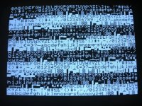
Commodore PET 2001 with no cursor

With the power OFF it might be worth double-checking that the RESET pads are wired to the correct place.

One RESET pad should connect to pin 40 of the 6502 CPU (/RESET).

The other RESET pad should be connected to GND (6502 CPU pin 1).

Check with a multimeter set to read resistance.

When you press the reset pushbutton, pins 1 and 40 of the 6502 CPU should be connected together with a low resistance. The resistance should be high when the pushbutton is released.

If this is the case, your RESET pushbutton should work...

Dave
 
As Dave says, best to check continuity to verify things are connected correctly.
The pad labeled RST on the romulator is connected to pin 40 on the 6502. The other pad on that header is connected to a 100 ohm resistor which goes to GND, which on the romulator is directly connected to pin 21 on the 6502. One thing to note - pin 1 on the 6502 on the romulator board is not directly connected to pin 21 even though both are ground pins. As I recall, this was to support a 65C02 which has a separate use for pin 1, so instead of directly connecting the two pins to the same ground on the romulator board, pin 1 just connects only to pin 1 on the mainboard socket, while 21 is connected to ground. In the case of the pet 2001-8, though, both pins are connected on the mainboard. This just means that it would make sense to check continuity while the romulator is connected to the PET 6502 socket.
 
if there's an issue having that 100 ohm resistor between RST and GND, there is another pad labeled GND on another unpopulated header near the RST header, you could connect between RST and GND directly that way.
 
if there's an issue having that 100 ohm resistor between RST and GND, there is another pad labeled GND on another unpopulated header near the RST header, you could connect between RST and GND directly that way.
All connections are fine, the connection across the 100 ohm resistor to pin 40 too, only the 100 ohm resistor seems to be the problem. I get a reset if I connect pin 40 directly to GND.
 
Ah ha... Found the culprit...

That's interesting, the PET 2001 uses the output from a 74LS04 to drive the /RESET on the logic. Effectively, the 100R pull-down resistor is competing with the internal pull-up resistor within the output stage of the 74LS04.

I often view this resistance to be in the order of 100 to 330 Ohms - so a 100 Ohm pull-down resistor may still be seen as a logic '1' (hence no reset).

This may depend upon a number of factors of course - the output of the actual 74LS04 gate on the PET and the input sensitivity of the 6502 /RESET pin.

It is generally safe to 'ground' the output of TTL gates.

Other PETs (e.g. the 8032) has a 1k pull-up resistor with an open collector 7417 driver. With this circuit configuration (1,000 Ohm pull-up and 100 Ohm pull-down) I calculate a Voltage of just under 0.5 Volts - which is guaranteed to be seen as a logic '0'.

Dave
 
Last edited:
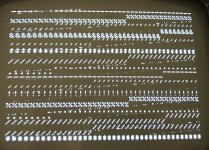
Excellent. That is the VDU check - and looks fine.

I assume it then moves on to the image in post #26? This is the page 0/1 memory test. If I get a few minutes between meetings I will analyse the image.

Of course, if you have a little bit of time to spare - you could have a look yourself.

The VDU screen indicates the PETSCII character set of your machine with increasing byte values from $00 to $FF.

This pattern is written into both Page 0 and Page 1 of RAM.

The first 256 bytes (of the screen image depicted in post #26) is either a 'G' or 'B' indicating a good or bad memory cell. The position (0..255) indicates the byte value written into the memory cell itself. $00 is written into address $0000, $01 is written into address $0001, ... , $FF is written into address $00FF.

If the first 256 bytes of the VDU screen indicate a 'Good' cell, then the associated character in the second 256 bytes of the VDU screen indicate a '.'. If a Bad cell is indicated, the character that was actually present in the memory cell (other than the one we were expecting) is displayed. By doing a 'reverse lookup' (to convert the character into a hex code) means that you can identify what was wrong. Repeat this for all 256 bytes of page 0.

The second half of the screen indicates the same information for page 1 of the memory. Well, for a 40 column PET - just slightly less than a full page!

You need to view this as a logic puzzle. What you are trying to find are 'common themes' (e.g. is it always a specific data bit - or bits - that are stuck at a logic '0' or '1'; is it always a group of bits - corresponding to a specific RAM chip; is it an address line that is stuck at a '0' or '1' etc.).

Dave
 
Harald,
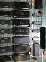
Please post a photo of the seven ROMs so we can get the part numbers and find the BASIC version toy have. We will have to verify the checksum numbers.
 
Excellent. That is the VDU check - and looks fine.

I assume it then moves on to the image in post #26? This is the page 0/1 memory test. If I get a few minutes between meetings I will analyse the image.

Of course, if you have a little bit of time to spare - you could have a look yourself.

The VDU screen indicates the PETSCII character set of your machine with increasing byte values from $00 to $FF.

This pattern is written into both Page 0 and Page 1 of RAM.

The first 256 bytes (of the screen image depicted in post #26) is either a 'G' or 'B' indicating a good or bad memory cell. The position (0..255) indicates the byte value written into the memory cell itself. $00 is written into address $0000, $01 is written into address $0001, ... , $FF is written into address $00FF.

If the first 256 bytes of the VDU screen indicate a 'Good' cell, then the associated character in the second 256 bytes of the VDU screen indicate a '.'. If a Bad cell is indicated, the character that was actually present in the memory cell (other than the one we were expecting) is displayed. By doing a 'reverse lookup' (to convert the character into a hex code) means that you can identify what was wrong. Repeat this for all 256 bytes of page 0.

The second half of the screen indicates the same information for page 1 of the memory. Well, for a 40 column PET - just slightly less than a full page!

You need to view this as a logic puzzle. What you are trying to find are 'common themes' (e.g. is it always a specific data bit - or bits - that are stuck at a logic '0' or '1'; is it always a group of bits - corresponding to a specific RAM chip; is it an address line that is stuck at a '0' or '1' etc.).

Dave

Hi Dave,
I've tried to solve the puzzle using an Excel spreadsheet, but haven't gotten any result so far. I keep trying...
Harald
 
Post #48...

The initial problems we see appear to be associated with three stuck ‘1’ bits in the least significant 4 bits of the byte. RAM I1 is responsible for this - so I would start there. The problem could also be associated with the buffers H8 and/or G5.

I assume your RAM chips are soldered onto the board? Or are they in sockets? Ah, just looked at your photographs, they are in sockets - yes?

You could try swapping RAM chips around, but before you do that we need to come up with a system of working so we don’t confuse the hell out of ourselves with randomly trying things! Again, another logic puzzle!

Dave
 
Last edited:
The initial problems we see appear to be associated with three stuck ‘1’ bits in the least significant 4 bits of the byte. RAM I1 is responsible for this - so I would start there. The problem could also be associated with the buffers H8 and/or G5.

You could try swapping RAM chips around, but before you do that we need to come up with a system of working so we don’t confuse the hell out of ourselves with randomly trying things! Again, another logic puzzle!

Dave

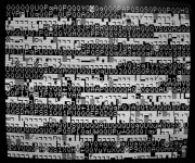
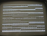
Referring to post #1 I assume the original garbage screen was entirely random in nature like the first image below. If so swap the suspect system chip RAM 11 with the video RAM chip in socket C3. This should be done without the ROMulator fitted and with the PIAs removed. If the PET displays a non-random character screen like the second image below then RAM 11 has stuck bits.

Alan

PET RAM Garbage.jpg PET RAM UC3 Fault.jpg
 
Referring to post #1 I assume the original garbage screen was entirely random in nature like the first image below. If so swap the suspect system chip RAM 11 with the video RAM chip in socket C3. This should be done without the ROMulator fitted and with the PIAs removed. If the PET displays a non-random character screen like the second image below then RAM 11 has stuck bits.

Alan

View attachment 1240825 View attachment 1240826

Hi Alan,
I swapped I1 and C3. Now it looks different.
Harald
 

Attachments

  • 0434878E-10DC-44AF-B25E-976BBC3CBC5B.jpeg
    0434878E-10DC-44AF-B25E-976BBC3CBC5B.jpeg
    1.2 MB · Views: 8
You definitely have a faulty RAM then (we don't get any G or B letters in the first 256 bytes).

The simplest way to test the RAM (in my opinion) is to proceed as follows:

1. Identify each of the RAM devices by a sticker (I1, I2, ... I7, J1, J2, ... J7).
2. Keep replacing I1 and J1 as a pair with other pairs of RAM chips until the page 0/1 RAM tests pass.
3. At this point you can observe what the ROM checksums are (note these down) and you can test the keyboard for operation.
4. Keep the devices that are in I1 and J1 safe (they are potentially good and you don't want to loose them!).
5. Keep replacing I1 and J1 with other pairs of RAMs and checking again for the page 0/1 memory tests to pass.

At this stage you should have a 'gold' I1/J1 RAM pair (the first good pair that you found), a pile of other working pairs, and a pile of non working pairs.

6. Put the original 'gold' pair back into I1/J1 and make sure that everything still works as it did before.
7. Remove the 'gold' I1 RAM (keep it very safe) and test each RAM in the 'non working' pile in socket I1. If the device works - it is potentially good. If not - it is potentially faulty.
8. Put all of the working RAM devices back into the PET from I1/J1 upwards in pairs.

If memory serves me correctly, my PETTESTER assumes a minimum of 4K of working RAM to run the full memory tests (8 RAM chips). I will 'correct' this in Version 5 to only assume 1K...

9. Test again. Hopefully your PET will still pass the page 0/1 memory test, and move into the full memory test and (hopefully) give all of the installed RAM a clean-bill of health.

10. Whatever 'dead' devices you have - decide what you want to do about them (e.g. replace with originals or whatever).

A word of caution... This involves a lot of RAM swapping, necessitating turning the power ON and OFF. This is not usually very good for a vintage PET! My suggestion is to do these tests slowly. Go away between testing each pair of RAMs and do something else - hoovering, gardening, painting a picture etc. to prevent too many ON/OFF operations in a short period of time.

That's my suggestion at any rate.

This all assumes the RAMs are in sockets of course.

Dave
 
Last edited:
My suggestion in post #53 and the example screen shots were put forward on the basis of running the machine without the ROMulator (ie, not PETTester either) with the PET in its original configuration (including the ROMs) but with the PIAs removed. It was just meant to be a simple way of checking RAM 11. Swapping chips and running PETTester at the same time just confuses me! All 18 RAM chips are socketed by the way.


Alan
 
All we are effectively doing with the PETTESTER with the page 0/1 RAM test is testing the two (2) RAM chips at I1/J1. We are testing no other RAM chips concurrently.

All I am proposing to do is to put a pair of RAMs into I1/J1 and turn the power on with the PETTESTER ROM in position.

It either passes the page 0/1 RAM test or fails it.

Dave
 
Hi Dave and Alan,
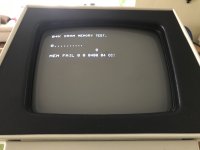
I1 was the bad one. All other RAMs seem good so far. I have repeated the test with the 7 good RAM pairs.
Harald
 

Attachments

  • 3DD704F7-5418-4D96-88B5-5EA243AE982A.jpeg
    3DD704F7-5418-4D96-88B5-5EA243AE982A.jpeg
    777.2 KB · Views: 9
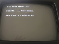
or I am wrong, this is what I see with one pair ROMs inserted. Good or bad?, thought the MEM fail means the missing 7 ROM pairs.
 

Attachments

  • B171BEFF-DA90-4CDC-A2F7-8239E0C01BA3.jpeg
    B171BEFF-DA90-4CDC-A2F7-8239E0C01BA3.jpeg
    1.6 MB · Views: 6
Last edited:
Back
Top