• Please review our updated Terms and Rules here

Cromemco dazzler replica project

All my test program does is to:

1. Enable the dazzler.

2. Set the display memory start to 0.

3. Permit you to set the bits of port 0Fh to whatever you want.

The dazzler will then display whatever is stored in display memory according to the bit settings in port 0Fh.

My test program doesn't actually 'do' anything to the display...

It basically performs the same function as the original Cromemco Dazzler test program when combined with the Cromemco front panel sense switches - but using the console port instead.

Dave
 
Last edited:
Oh wow.. look what I found when I removed IC34.. 😭
View attachment 1276809
That sort of thing is not uncommon when a lot of chips are getting fitted, I found one like that in my SOL-20.

It would be worth a quick visual inspection to check all the other IC's , just in case there is another one like this.

I remember when I first powered my Dazzler I was somewhat surprised that it worked properly first time (and that is despite having those two pull ups not connected to +5v) because of the large number of IC's and steps involved. I think there was an elementt of luck in it too, though I did go to the ends of the earth to find vintage genuine vintage IC's which helped.
 
I look at the rows of pins on the ICs horizontally against a bright light. I can then generally see any bent pins like this tucked under the body of the IC.

Does anyone know what the last modification is to the REV C board described in the Cromemco Dazzler Games manual?

They move the input to IC49/1 (and I suspect all of the other buffers) from IC57/12 to IC57/11. It has something to do with the S-100 bus floating and DMA accesses (exactly what we are doing/observing here - possibly).

Dave
 
It would be worth a quick visual inspection to check all the other IC's , just in case there is another one like this.

Just got some chips from Don & am due some more from eBay tomorrow. I'll be sure to inspect everything when I start pulling chips.
 
The plot thickens...

So we get random data when we are not latching anything into the latches (IC47 and IC55), but when we need to latch some data into the latches, we always latch a logic HIGH in...

I suspect this logic is working - it is just that something is going wrong with the DMA cycle(s).

Can you also check what is happening at IC49 pin 1 please.

Dave
 
So that is all good.

All of the S-100 bus buffers between the Dazzler and the memory are enabled well in advance of when they are actually needed.

OK, bed time in the UK...

I think we need to have a look at the DMA address next, to ensure that the correct memory is actually being addressed.

There will be something stupid somewhere, we just have to hunt it down in a logical manner..

we could also remove a couple of ICs and 'force' the data bits to display a coloured screen. Let me think about this one...

Dave
 
I have already ordered some NOS replacements, should have it early next week.

Anyone have a good tester they can recommend?

I have this one

https://www.aliexpress.com/item/1005003579455285.html? but it doesn't seem to be widely available now

but these are and have a full screen rather than a single digit 'morse code' type of display. I imagine they are just a later version of the same thing and use the same library.


Not tried these directly.
 
The problem with all of these is the lack of documentation related to the test vectors that are used to check a device - or the percentage of test coverage.

We have previously identified that some pins of a couple of 74 devices are not tested with certain testers.

I had the same issue with one of our repair companies we use at work. We had a fault on a board. They plugged it into their test rig, and it passed.

When I had a look at the test rig, it didn't actually test this input signal!

Once I had explained to the test engineer what this input actually did, he was able to modify the test vectors to test this input and, lo and behold, the card failed this time.

A bit of poking with an oscilloscope and we found the faulty package and the board was working once again.

Of course, this meant that all the boards of this type that had been previously repaired/tested had not had this input signal (or the associated logic) tested either.

Just a warning not to believe any piece of test equipment at total face value (especially at the budget end of the market)...

Dave

the "Lack of documentation" remark is very telling.

A good example of this is the TTL IC testers on ebay which claim to test 74 series IC's.

The designers of some of these need to go back to school in a time machine and get a lesson from an Engineer at Texas instruments back in 1969. The engineer had pens in his pocket and a suit, with a thin black tie and a white shirt and generally always carried an HP calculator, like the HP-25 (with RPN).

The modern conceived tester protocols could not imagine a chip like the SN7425, it had a control (strobe ) pin, that enables or disables the gates withing the package. A lot of TTL IC's had such strobe pins, with input current levels that were not like a single TTL input pin.

The strobe pin is enabling or disabling 4 of the inputs to each gate in the SN7425, not one, the current sinking on that pin, to create a logic low is x4 the normal value for a 74 chip TTL input.

The tester is "not prepared for this" and reports the chip as defective. However, because 74LS series chips (or HC, HCT etc) have lower input currents, the tester, likely tests these as ok. When in reality both are ok.

Other testers I have bought for testing Memory chips in vintage computers have been equally as disappointing. Malfunctioning and declaring higher speed chips as failed when they are perfectly good.

What I'm saying here is that you can take a lot of modern IC tester results, with a grain of salt, especially if they have been programmed on devices like Arduinos by latter day Engineers, who did no grow up with with the 1970's style TTL technology, because there are many nuances that they are oblivious to in this vintage tech, and sooner or later, that will catch them out. They can still be excellent programmers though, no dispute there.

If you could find a TTL IC tester made in 1980, it might be another story and give you reliable results.

Still, I generally I don't bother with IC testers for standard 74 series TTL's because, it is actually better to check them in circuit, with the scope, to ensure they are obeying their logic table. This is testing them in the circuit they were designed to run in and were known to run in, in my view it is mainly the better test method for these vintage parts.

Still, when it comes to IC testers, in my experience at least, it is more likely they will test a good parts as failed, rather than the reverse. So it is interesting that your IC tester, tested the 74157's as ok. So, despite being counterfeit, they are possibly ok functionally.
 
Last edited:
Back to the dazzler...

I have re-checked all of the traces you have taken for me and I find no discrepancy with any of them. They all appear correct.

Next is to move on to the DMA circuitry for the dazzler to access the memory.

When IC49/1 goes HIGH it basically means that the Z80 CPU has been forced off the S-100 bus and the dazzler is going to take over control of the S-100 bus itself.

Setup the test as per our 'standard' configuration:

Use RDOS to place some 'random' data into memory addresses from 0000 to 001F (say). Let's make sure there is some data in video memory to work with.

Run my test program and set the data bits D7 to D0 of port 0Fh to '00011001' (normal resolution, picture in 512 bytes). D5=0.

Test point 'T' as a trigger at the correct timebase setting (5 us/div).

Measure IC49/1 and look at when it goes HIGH in relation to the 'T' waveform. Remember the point in time at which it goes HIGH. After this time is what we are largely interested in for the following measurements:

Check the following pins for a logic HIGH:

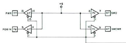
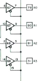
IC67 pins 5 and 13.
IC70 pins 7 and 9.

1711811231802.png
These four pins drive some of the control signals on the S-100 bus.

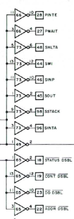
There are a lot of other control signals that are also driven. You can check them on the OUTPUT side of the inverter buffers if you like. They should all be LOW (e.g. IC66 pins 10 and 4) after our IC49/1 goes HIGH of course:

1711811171835.png

If these test out OK, we can then move on to look at the address counters... See my next post for this.

Dave
 
As a continuation of the above, but this time looking at what address is being sent out by the dazzler.

This is all valid AFTER the time IC49/1 has gone HIGH again (as per the above post).

These are the first four (4) address lines A0 through A3. The should count from '0' (0000) to 'F' (1111) during each interval of 'T' going HIGH. A0 should be twice as quick as A1 and so forth to A3 (slowest).

1711811482883.png

Below address A3 (on the schematic) are more address lines (A4 to A15).

1711811677833.png
We need to check each of the buffer outputs as well.

Now, a 512 byte video picture (based at address 0000) should cycle from addresses 0000 to 01FF. Therefore, A0 through to A8 should be oscillating as a binary counter. You will have to slow down the oscilloscope timebase to see the higher address lines changing though. Try your best...

Address lines A9 through A15 should all be LOW.

See how you get on with that...

Dave
 
Post note.

You may find it easier to check the INPUTS to the address bus buffers FIRST (e.g. IC67 pin 6). Do all of the inputs (adjusting the timebase accordingly).

Then, after checking all of the inputs to the address bus buffers, make sure that they are transferred to their outputs (when IC49/1 is HIGH). You just need to make sure that within the period just after 'T' goes HIGH (with a slight delay occurring to account for when IC49/1 goes HIGH) that the address line transitions both HIGH and LOW.

Of course, address lines after A8 should all be LOW anyhow...

Dave
 
So I got a bunch of vintage chips in from Don & Ebay.. swapped a total of 28 chips today and I still have no color running GDEMO, and from what I can tell - no difference. So disappointing (and expensive! but I knew that going into this) lol .. will proceed with these tests.
 
If all the dazzler is doing is reading data bytes of 'FF' from the S-100 bus (irrespective of what is stored in RAM), then all that will give us is a picture of a bright white cat in a snowstorm irrespective of what chips are installed.

Dave
 
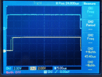
Measure IC49/1 and look at when it goes HIGH in relation to the 'T' waveform. Remember the point in time at which it goes HIGH. After this time is what we are largely interested in for the following measurements:
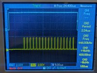
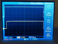
Check this out, this is the pin 49/1 reading from today. I do see the voltage was much higher (~5V) before, compared to about 3.8V now. I'm assuming this is more in line with what vintage chips would produce?
ezgif-4-e3d1543153.gif

ok, proceeding...
 
Back
Top