Hugo Holden
Veteran Member
Fantastic stuff! I'm curious about the process of using Picture IT - I'm not familiar with it.. are you basically tracing over an original layout image? And then cutting and pasting things like pads, etc? My tactic has been to download whatever I can get my hands on into photoshop, convert to B/W, and then clean up with manual brush work. I did that to recreate an SWTPC PPG joystick PCB, using just the parts layout diagram from their manual (all they supplied) to 'reverse engineer' it.
Basically I use the original board track layout from the book image or from a photo of the pcb. If you look at the bottom of page 3 in this article, you can see an image of drawing over a photo (without the grid) on a pcb, this is why the tracks look red in color:
www.worldphaco.com/uploads/Personalityreplica..pdf
If the board photo is not taken square on aspect (often the case), I use Photo Studio 4 to fix that as it has an aspect ratio corrector for a tilted image. But I find Picture IT much easier for general drawing , so I use that rather than PSP4.
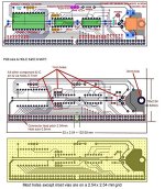
Using the transparency option I place a 2.54mm grid over that, so I can see both images at the same time and align this with the IC pads. I m most cases the original designers laid these boards out on a 2.54mm grid and sometimes even the vias fall on regular places between these, but that is somewhat variable. Then I trace over that. Also it is a matter of having everything in proportion. The IC footprints effectively generate the scale and the board perimeter must be specified.
If you look at the attached image of another board, you can see how a 2.54 mm grid is helpful as it can also be used to specify the board perimeter if that is a multiple of 2.54mm.
Those Dazzler images were very close to Cromemco's faded ones. But one important thing, for an S-100 card is the exact board perimeter geometry and the position of the fingers must be bang on. It was found when my images (essentially Cromemco's touched up images) were overlaid on the standard s-100 board image, the position of the fingers were not exactly correct, this was a small error in Cromemco's foil diagram geometry. So that got corrected before the boards were made.
Also, something that gets overlooked sometimes when you see projects where pcb's have edge connectors designed to plug into a socket, for example S-100 boards or SOL personality modules etc, it is important that the leading edge of the pcb toward the fingers has an initial taper and that the corners of the rectangular edge of the pcb projection with the fingers are slightly rounded, to assist & guide the entry of the card edge into the socket with minimal initial force. This is kinder to the socket otherwise there is a high initial force and an abrupt entry into the socket, which doesn't sound very romantic either. This extra machining is more work for the pcb maker of course, adding to the price, which might be why some pcb quotes look cheaper too, the Devil is in the detail. I also use mx-3 to lubricate the edge connectors & sockets to avoid wear on all my s-100 boards & SOL-20 sockets, PET GPIB connector etc.
Like I say its all very old school image drawing, but it works.
There was a thread recently where Gerbers were made from my .jpg images in my RM-65 video card article, that was a fun one, being a compact 4 layer board and trying to figure out the two internal layers. Maybe if we found out how that was done, what process was used to make the Gerbers, it could be helpful. I'm not sure where that thread is right now.
Attachments
Last edited:
") ...
...