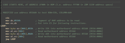
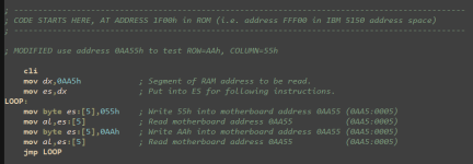
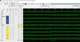
Ok wrong heheh. I can see the code will have to look more like TEST5066. During my study I remember seeing physical address generation, offset & segment registers. Will need to revisit that, probably something you pros incorporate automatically 
Upcoming Events:
- VCF South West - June 14 - 16, Davidson-Gundy Alumni Center at University of Texas at Dallas
- VCF West - Aug 2 - 3, Computer History Museum, Mountain View, CA
- VCF Midwest - Sept 7 - 8 2024, Schaumburg, IL
- VCF SoCal - Mid February 2025, Location TBD, Southern CA
- VCF East - April 2025, Infoage Museum, Wall NJ
-
Please review our updated Terms and Rules here
- Forums
- Companies
- IBM Computers, PCs, Clones and Descendants
- PCs and Clones (XT and early AT class machines)
You are using an out of date browser. It may not display this or other websites correctly.
You should upgrade or use an alternative browser.
You should upgrade or use an alternative browser.
Fixing Five Festive 5150 Boards over the Holidays (BOARD #3 Thread)
- Thread starter VeryVon
- Start date
Last edited:
modem7
10k Member
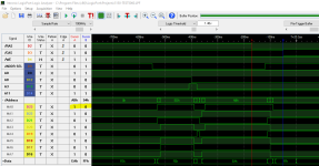
Regarding the first shown capture, showing the portion where AAh is written to address 55AA.Ran a capture of 55AA. ROW is 45h (bit 3 out of sequence) and COL is 2Ah (bit 0 out of sequence)
BYW: Your A cursor (ROW) should be slightly to the right, in the area where the data is shown as AAh. Just a technicality. As you can see, it doesn't affect the ROW address seen.
I presume the ROW address is displayed as 45h rather than A2h due to your choice of LA wires. So, yeah, that highlighted 0 in cursor A should be a 1.
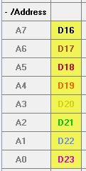
Here's what the actual mapping is. I think I have the captures reversed because in the images above the group data format is "Wire MSB -> Data MSB" ... should be "Wire LSB -> Data MSB"?I presume the ROW address is displayed as 45h rather than A2h due to your choice of LA wires. So, yeah, that highlighted 0 in cursor A should be a 1.
modem7
10k Member
You have used ascending wire numbers on descending address bits.Here's what the actual mapping is:
I have done that myself. There is an option somewhere, where you can get the software to cater for that. Try right-clicking on "-/Address" and seeing what is available.
Ok yep, I think I found it. "Wire LSB -> Data MSB"You have used ascending wire numbers on descending address bits.
modem7
10k Member
Yes, although the chances of the resistor network being the problem cause are really really low.This suggests a problem with U62 and/or RN4?
For the ROW address, you are seeing A2, not AA, i.e. bad bit 3 in the ROW address.
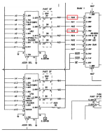
Refer to the diagram at [here].
Bit 3 in the ROW address corresponds to A3.
Per the diagram, A3 is routed through U62.
Time to swap out U62.
I pulled U62, and two LS158's from the donor board. They all test out OK on the chip tester. Socketed U62 and tried with both donor chips, RDR has same error. Disappointing, but we continue.
p.s. I also verified the resistances across RN4.
p.s. I also verified the resistances across RN4.
modem7
10k Member
Hmm. I need to have a decent think about this (in amongst other stuff I'm doing). I will probably do my own capture.I pulled U62, and two LS158's from the donor board. They all test out OK on the chip tester. Socketed U62 and tried with both donor chips, RDR has same error. Disappointing, but we continue.
p.s. I also verified the resistances across RN4.
While I'm doing that, a couple of suggestions:
- Remove the (known-good) RAM chips from bank 0, and see if that changes the capture.
- For the problem bits, add the 'address bus' version to the capture, i.e. verifying that the source address to U65 is correct. (Yes, you verified the address bus earlier, but is something else going on, e.g. bad code out of TEST ROM.)
modem7
10k Member
I wrote some code, then did a logic analyser capture. All as expected. I have added it all as TEST5067 at [here].Hmm. I need to have a decent think about this (in amongst other stuff I'm doing). I will probably do my own capture.
By chance, you didn't accidentally put the bad 74LS158 back in ?
I don't think so. I have 3 158's here. Two are from the donor board, the one from this board has a big "X" written on it with a sharpie. All of them test out OK on the chip tester.By chance, you didn't accidentally put the bad 74LS158 back in
Cool!I have added it all as TEST5067 at [here].
Ran capture with TEST5067. Below is what I typically see with RAM in there. I still have to setup a test where I remove the RAM chips. I'm starting to feel like there's something electrically faulty in the ram bank, but close examination under the scope hasn't revealed anything obvious.
p.s. ADDR SEL, A0, A3, A8 & A11 are read directly off U62. I also checked the grounds and power on U62, looks ok.
READ55AA:
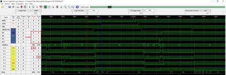
READAA55:

p.s. ADDR SEL, A0, A3, A8 & A11 are read directly off U62. I also checked the grounds and power on U62, looks ok.
READ55AA:

READAA55:

modem7
10k Member
Consistently bad MA0 and MA3 outputs out of U62, with good corresponding address bus inputs.
- Known good U62 chip.
- RAM chips removed in case of some strange loading problem for U62.
- RN4 partially checked.
- PCB status unknown.
- Some confidence in power to U62.
Re my "RN4 partially checked." above. You didn't write that you ensured that all resistors were isolated from each other. Ideally, RN4 would be removed from circuit, and a multimeter used to verify that each resistor has infinite resistance (or maybe many megohms) to the other resistors.
So how about you just home in one anomaly, MA0. You have U62 socketed. In a capture, does MA0 behave as expected if you lift the U62 leg connected to MA0, and have the probe on the lifted leg? If so, the problem cause surely has to be something 'downstream' of U62.
Yea, I definitely didn't scrutinize RN4 enough. I'm getting 30 Ohms between pins 3 & 13?? (yes 30 Ohms!)
Ok, MA0 & MA3 are shorted together somewhere. Looking...
EDIT: most of the routing for these signals takes place on the top of the board. Afraid I might have to remove all the bank 0 sockets to see if it's under there.
EDIT: most of the routing for these signals takes place on the top of the board. Afraid I might have to remove all the bank 0 sockets to see if it's under there.
Last edited:
modem7
10k Member
Presumably, you removed RN4 to see if it was the problem cause.Ok, MA0 & MA3 are shorted together somewhere. Looking...
EDIT: most of the routing for these signals takes place on the top of the board. Afraid I might have to remove all the bank 0 sockets to see if it's under there.
Correct!Presumably, you removed RN4 to see if it was the problem cause.

