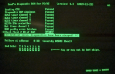
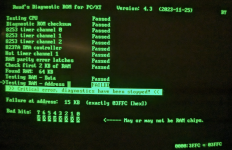
When running test 5066 shouldn't we see some RAM refresh on RAS?
Upcoming Events:
- VCF South West - June 14 - 16, Davidson-Gundy Alumni Center at University of Texas at Dallas
- VCF West - Aug 2 - 3, Computer History Museum, Mountain View, CA
- VCF Midwest - Sept 7 - 8 2024, Schaumburg, IL
- VCF SoCal - Mid February 2025, Location TBD, Southern CA
- VCF East - April 2025, Infoage Museum, Wall NJ
-
Please review our updated Terms and Rules here
- Forums
- Companies
- IBM Computers, PCs, Clones and Descendants
- PCs and Clones (XT and early AT class machines)
You are using an out of date browser. It may not display this or other websites correctly.
You should upgrade or use an alternative browser.
You should upgrade or use an alternative browser.
Fixing Five Festive 5150 Boards over the Holidays (BOARD #3 Thread)
- Thread starter VeryVon
- Start date
modem7
10k Member
No.When running test 5066 shouldn't we see some RAM refresh on RAS?
RAM refresh is something that needs to be initiated via code. It's one of the things that the IBM POST does. The RAM refresh mechanism only needs to be initiated if values are to be stored in dynamic RAM, and then those values read back (undamaged) after quite a delay. TEST5066 does not do that, and so there was no need for me to put 'Initialise RAM refresh mechanism' code into TEST5066.
Even the following does not need RAM refresh to be initialised. Why. Because the act of reading address 0 refreshes address 0.
1. Write AA to address 0.
2. Read address 0, verifying that contents are AA.
3. Jump to 2. (2, not 1)
modem7
10k Member
Yes, because you have an addressing problem,and you are now satisfied that the address bus is fully functional.Should we look into the address multiplexing logic now?
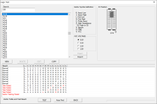
Note the following, part of the capture PNG file within TEST5060.ZIPEDIT: Ok yea, let's go back to [TEST5060]

So TEST5060, as written, does not test the address multiplexing.
You need to modify the test motherboard address used from 0 to something that:
- Is still within the bank 0 range of addresses (so you know which bank to put the probes on), and
- Results in a row address that is different to the column address (something that you will see in the capture).
Ideally, a motherboard address that results in ROW=55h, COLUMN=AAh
Then change the address so that the opposite happens: ROW=AAh, COLUMN=55h
modem7
10k Member
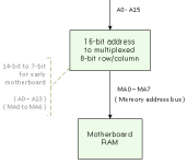
I decided to create a diagram - see [here].You need to modify the test motherboard address used from 0 to something that:
- Is still within the bank 0 range of addresses (so you know which bank to put the probes on), and
- Results in a row address that is different to the column address (something that you will see in the capture).
Ok perfect, that's extremely helpful.I decided to create a diagram - see [here].
So if I follow the diagram correctly, we can use:
055AA hex to test ROW=55h, COLUMN=AAh
0AA55 hex to test ROW=AAh, COLUMN=55h
modem7
10k Member
RAS has to be there - the 'Testing RAM - Data' test of RDR passed.RAS appears to be stuck high.
Does that test now fail?
Ok perfect. If I trace that back, I see a RAS pulse at U81 pin 2, but DACK 0 is always low.If we look at the diagram at [here], that suggests a problem with U65 or U49.
modem7
10k Member
DACK 0 is part of RAM refresh.Ok perfect. If I trace that back, I see a RAS pulse at U81 pin 2, but DACK 0 is always low.
For the RDR ROM, the RAM refresh mechanism does not get initialised completely until step 55 at [here].
For the TEST5060 ROM, the RAM refresh mechanism is never initialised.
There are two types of /RAS:
- Those, where one happens every approx. 15 us, as part of RAM refresh; and
- Those that happen when RAM is read or written - kind of a 'normal' /RAS.
With the TEST5060 ROM in, and the target address being somewhere in bank 0, then you are expecting to see 'normal' /RAS directed to bank 0.
The RAS pulses will pass from pin U65-6 to pin U65-11 when all of the following are true:
- Pin U65-4 (DACK 0) is LOW. (I.e. a DMA refresh cycle in not in progress.); and
- Pin U65-5 (/ RAM ADDR SEL) is LOW. (I.e. Asserted to indicate a motherboard RAM address.); and
- Pin U65-1 (A16) and U65-2 (A17) are both LOW. (I.e. A motherboard RAM address somewhere in bank 0.)
modem7
10k Member
There are never any guarantees with that technique.I do have a known good LS138 here, I tried the piggy-back technique, but no change.
At the time when /RAS is expected, a tug-of-war could be happening on pin 11 between the soldered and piggybacking U65, with the soldered U65 winning the tug-of-war.
Agree. I'm going to pull the chip out and put it on the tester.tug-of-war could be happening
modem7
10k Member
Out of interest, what is the make-model of chip tester that you have ?Looks like we have a winner (or loser depending on how you look at it)
XGecu T48 [TL866-3G] Ver: 00.01.30what is the make-model of chip tester that you have ?


