• Please review our updated Terms and Rules here

Homebrew TVT I picked up

I remember using one of those same Radio Shack PCBs. One problem that I found is that unless the board was scrubbed with Scotchbrite before soldering, it was difficult to get solder to stick to the traces. Checking all of the connections might be a good idea.

Nowadays, of course, if I need a bit of protoboard, I'll buy the FR4 stuff with tinned traces and plated vias. That's one thing that has improved over the decades. Vector-branded prototype boards were a bit on the expensive side.
 
I think my problem may in fact be the video board. I noticed when I look at the 'random' garbage onscreen when it fires up, that it actually has a repeating pattern to it.. ie a line will have a random pattern of say, x number of characters, and then that will be followed by a copy of that same pattern over again.

I took a look at the 7495 shift registers. I notice when I pull one of them, I get a screen full of 1s, except for two columns that are a mirror of each other with totally random characters. I might be wrong, but I feel those columns might be a hint. Swapping the two chips around doesn't change anything though.

Something is causing repeating patterns and when the 6800 is sending data it is shoving duplicates of the incoming data into two columns. I don't know why nothing comes up on the right half of the screen.. I'm guessing the 6800 was designed for 32 characters so perhaps if this TVT were working right it'd basically only use half the screen.

I'm about as certain as I can be that it isn't RAM. I have tested and retested the RAM in other machines, and even borrowed RAM from those machines.

Man I wish I understood circuitry better. I'm really trying!
 
The scan and character addressing is driven by counters. Suspect those first.

Very often, new characters are added by waiting for a count to come along, so look for comparator circuitry.
 
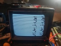
Thanks Chuck. This is what the output looks like with one of the shift registers pulled:

20190629_215121.jpg

I don't know if it means anything. But I find it interesting the whole screen goes to one thing except those two columns on the right. And those slowly change to almost resemble the rest.

I don't think it's a bad socket thing.. I pressed on the ICs to see if anything changed.. nothing did. I'll try and figure out the connections between them tomorrow.
 
Those two columns on the right are the same distance apart as the repeating columns on the left, aren't they?

What do you mean the screen goes to one? Do you know that the '$' character is value 1? If so, this is significant; it means that data bit 0 is stuck on. I find that a little confusing though; 'B', 'b', or maybe '!’ is more likely to be 1 in my opinion.

I don't know how the display is stored in your device. I've seen a small handful of designs for these things. So I'm not sure what the shift register that you pulled does. Is it character storage? I think not because your bad columns don't repeat enough, and don't move. But this shift register must be before the character generator, as complete characters are formed. What happens if, with that shift register removed, you shunt it's output pins (at the socket) to ground?

It seems to me more like the characters are stored in SRAMs, and that you have both a data and address problem at that RAM. It may be as simple as one stuck bit each. But then something else is causing the bad characters in those two columns. Noise? Or just a bad RAM chip (or connection to it)?
 
I have tested the RAMs repeatedly in my digital group video cards... cannot discern a problem. I suspect bad connection someplace, given the abundance of chip rust in some areas of the board. I am just trying to come up with a plan to deduce where the offender is.
 
Just did that... same thing.. repeating pattern.

I did a logic probe on the A0-A9 pins on the 2102s. There is clock signal on all except A9 (pin 14). On that one, my probe just indicates a solid 'low'. That is the same on all of them.
 
Just did that... same thing.. repeating pattern.

I did a logic probe on the A0-A9 pins on the 2102s. There is clock signal on all except A9 (pin 14). On that one, my probe just indicates a solid 'low'. That is the same on all of them.

Same two columns of not-similar characters?
 
I think so.

I'm actually working on tracing it all out. It seems the 2102 address pins all connect to 74157s, except pin 14, and pin 8. As mentioned pin 14 goes to a 74LS00, so I'm guessing that only gets triggered for special purpose. Pin 8 is A0, maybe same thing? I cannot find a connection to pin 8. I've made a Photoshop version of the back of the board so I can more easily trace wires (PSD format) here:

https://drive.google.com/file/d/1kDZJ2Sm05TKaAksMCSwNADdi7yjLDvzE/view?usp=sharing

I used PSD format so I could turn the labels (layers) on and off to follow wires. I'm going to do my best to document as much of the circuit as I can. Pin 8 is bothering me. I think I can see it going to one of the 74157s, but there's no continuity there. Given those two sockets suffered some serious rust damage, I'm thinking maybe (maybe) I'm on the right track.
 
Try to think functionally here. It will save you hours of random debugging.

The 74157 is a quad 2-input mux, so it's used to switch between two inputs. So what would those two inputs be?

Well, you have the screen refresh going on all the time. That's one. And then you have writing to the display RAM (2102), which would be another. Thus, the select (pin 1) of both 157s should pulse low every time you write to the display, but otherwise not. Pin 15 (enable) should always be low, as there's never a time when you're not driving the 2102 address lines.
 
So I've traced the pins, per this diagram I've made:

https://drive.google.com/file/d/1kn92zbKhhyWOp9Z2TJ3CAvYBL44N_VGU/view?usp=sharing

Almost all the memory address pins can be traced to one of the two 74157s. The exceptions are pin 14, which goes to a 74LS00, pin 8, which goes to pin 6 of a JM385107/001BCB (no idea what that is), and then pin 16, which appears to be attached to nothing... I cannot find a wire leading from pin 16 to any other IC.. it seems like all the pin 16s are just tied together and that's it.

I did find a 'broken' wire coming from one of the 2102's pin 2 (I think.. hard to see). I don't see any evidence it was connected to anything, too short. I'm guessing this wire was just abandoned/clipped for some reason. Pin 2 of the 2102s definitely have a connection.

Anyway, I defer to those of greater experience on the meaning of all this.
 
OK, lets see what I can suggest. First lets see if we can isolate a few things and then run some test.
First what is going on.
First, how the dang thing works. Looking at the screen, you have 64 characters wide by 16 lines. That is 1K bytes of data. The RAMs are one bit wide so likely have one bit of each character for each address location of each RAM. The full width of RAMs would have the full character for one address. The output then likely go to A0 to A6 of the MCM6571A ( the font ROM ). The character on the screen is created by bits from the ROM. Each bit is access by ROW and column( look at the data sheet for the ). With each count of the RS0 to RS3, it produces one complete row of, of one character, to the D0 to D6. These bit would need to be serialized to the video out. I suspect that is one of the parallel in to serial out shift registers. It could also be done by a 8 to 1 mux but this would require a faster access time of the character ROM.
I suspect the shift register. Each row is sequentially accessed for each horizontal sweep each row of the RS0 to RS3.
It looks like this part of the circuit is basically working as we get a $ for most of the characters. The shift registers are likely working fine.
The fact that we see a constant row of $ with about the last 22 characters are different leads me to believe that at least 1/2 of the RAM is being accessed during the display sweep. It is most likely that were are seeing some part of the RAM. I then suspect the issue may be related to the writing of the RAM. In order to access the RAM, independently of the video sweep, we need some way to have different addresses for the write and for the read. For this, there should be mux input for the 10 address lines going into the RAM. I suspect that is the purpose of the 74157s. There are two possibilities here. One is that it waits for the vertical retrace to update the typed character. This is unlikely. Next is that if there is an incoming character, it just takes the address away from the video and writes the character ( typically done on many early videos ).
I will repeat, you need to connect the serial out to the serial in of the TVT. You can keep the clock and ground hooked up to your CPU but we really need to control the data going in more directly.
When you type ca character, we should be seeing pin1 of the 74157 toggle and see pin 3 of the RAMs toggle.
Check that and report back what you see( also is there any change on the screen? )
Dwight
 
Found pin 16.. connects to one of the 74157s. As far as I can see, the connections are all good.

To further my own learning, I bent out each of the 75157 output pins that go to the memory, one at a time, to see what the result was. When I bent out pin 12 on the left most 75157, instead of having two columns of repeating junk, I had four. Gonna dig around a bit more.
 
Thanks Dwight. I'll try to wire up the connector as you said and just use the 6800 to generate the clock.
 
Okay, so I wired the clock and ground to the 6800, and tied R0 and R1 together , unconnected to the 6800 MP-S. Here is the result.

https://youtu.be/GNOkHlQKJe0

The strobe on this keyboard is a bit weird. You'll hear two clicks of the keys for every space created.. for some reason I have to hit space bar, then hit a different key (like 'I') in order to then hit space and get another space again. Simply hitting space repeatedly doesn't work... it's like it wants to see different data before it'll strobe. Anyway, you can see what happened as I continuously did this. About the middle, I tried experimenting with hitting the space bar multiple times, but gave up and resumed hitting space and then another key to go all the way across.

And Pin 1 of the 74157 and pin 3 of the RAMs pulse as things are typed in.
 
Last edited:
Okay, so apparently that part is working. If you have the screen duplicated left-to-right as shown, the counters are suspect.

Let's see what has to happen to the data once it's into the 2102 RAM.

Mind you, I don't have a schematic in front of me; I'm just going from the standpoint of "How would I do this?"

Pin 12 of each 2102 is DATA OUT. You should be able to briefly ground pin 12 of each SRAM and see all characters on the display change.

If you've verified that, the next place for the data to go is into the character generator, so trace out the data path to the 6571. Does it go through a 1702?
 
All characters change eventually with each pin 12 grounded, but not all change when any individual 2102 pin 12 is grounded.

I am following the data path but I don't see anything that leads me to believe a 1702 is involved. I can disconnect the link between the video board and the boards that have the 1702s completely and still have characters onscreen.
 
Looks like some problem in the keyboard. We can go back to that later.
The second to the high order bit of the sweep address from the keyboard counter is not working. The character counter is working because we see the cursor moving all the way across the screen. This is done by a match of the counter and the current counter of the sweep counter.
This is progress!
Assuming, the builder didn't play with the addressing to the RAM, a line of text would be from A0 to A5 ( 64 locations )( It is possible to have that address lines swapped at the RAM as long as the inputs to the 74157s were correct. Hopefully he didn't do that so we can assume addressing A0 to A9 ). We need to know what the steady state of pin 1 of one of the 74157 is when there is no key hit.
From that we can determine the path to the input counter.
If we follow A3 and A4 from the RAM back to the correct counter. One counter will be for the character on the video and one will be for the character coming from the UART.
Since A3 looks to be working, lets follow that one first. A3 of the RAM is pin 6 of the RAM. Your drawing shows that path as to the right '157 in your drawing pin 9. That comes from the '157s pin 10 or 11 ( pin 1 = 1, pin 10 ). Follow that wire to its source. It should be a counter or a buffer to a counter.
Now lets follow the A4 ( the broken one ) from RAM pin 7 to the '157 pin 12. It should be from input pin 13 or 14 of the same '157 ( pin1 = 1, pin 13 ). I suspect this wire is broken or this '157 is bad.
Dwight
 
Back
Top