• Please review our updated Terms and Rules here

IBM 5110/5100 video Display card repair (possible diode fix)

Pin 2: a 108-ohm pull-up with no apparent output is odd. That's a very small resistor for a pull-up, too!

I may have that slightly wrong - those two resistors might be in parallel instead of series. But either way, agreed, seems odd.


Pin 6: wonder if there's a missing pull-up somewhere?

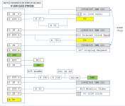
Nay, you caught a mistake! Thanks. The path for "H" does go *under* that IBM chip, but it actually doesn't connect to any pin of that chip. I searched further, and that PIN 6 actually corresponds to Display D07 (which is Display Request). Here is the revised report... (note that P05 ALARM is added in the expected and "measured"/observed location)
1656394147011.png

In the Excel chart, this "H" (my markings) connects with cell G42.


Pin 10: I am surprised to find the +6V reference connected to the driver IC --- it's not really connected to anything on the schematic...

Oh - it's connected to "Display Alarm On/Off Control". I assume this then meant that the IBM 2462314 tincan performs that Display/Alarm Control logic on the 5110?


(How did you manage to record from Pin 3?)

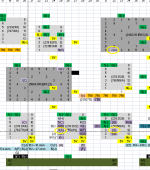
Well... I used black electrical (non-conductive) tape to masks off all the pins except two. Based on the continuity testing from earlier, I noted that that PIN3 is connected to those two additional locations on the back of the card (that I had marked with "A"). With the Language ROS out of the way, I get about 1-fist size amount of room to work with behind the card. Since the card is inserted without its support bracket, I placed cardboard between the cards to temporarily act as a support (and to keep from accidentally pushing the Display card component side over to the BaseIO card next to it). I didn't test PIN3 itself directly, since those lower pins are harder to access. But I monitored the two other pins that I found PIN3 had continuity with (since those two pins are along the same column, masking everything else with the electrical tape was easy).

Here is a focused view of the area, with the two pins of interest being yellow-circled in column 32.
1656395144885.png

With that practiced, and getting the same result across both cards and the two pins in that column - I was more confident at just testing the pin coming out from the 2nd pad in on the IBM tincan chip itself (since it is closer to the top of the board and easier to access). i.e. I tested it all again with no black masking electrical tape, and was practiced enough to just hold the jumper pin on the correct pin at the backside of the IBM tincan chip (the higher yellow circle in the image below).

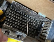
I think all that works, at least for comparing "BAD" vs "GOOD" cards. When the new scope arrives, I'll probably do the masking again, and focus on just PIN3 itself. Just those lower pins, I may need a (plastic) mirror also to ensure I'm hitting the expected pin, so it gets a little harder.
IMG_2758 - Copy.JPG
 
is the video signal feeding the VDU, it may have corrupt or absent H syncs and that may lead directly to where to look for the fault on the pcb.

The original problem was the fact that the bad card causes a PROCESS CHECK fault. It's possible that a component failing this close to the VDU would also send trouble in the opposite direction --- all the way back towards the data/address buses essentially --- but do you think this is likely?

If not, this may still be a worthwhile project to solve. But doesn't the bad Display Card still produce a good picture in single-step mode up until the fourth time you press the STEP button? As in, it would pretty much show a good, steady picture all day long in that configuration, as long as you never went through four steps?

PIN 6 actually corresponds to Display D07 (which is Display Request).

Interesting. This might be a worthwhile pin to probe and compare. It's possible that a Display Request at the wrong time could cause a PROCESS CHECK?

Oh - it's connected to "Display Alarm On/Off Control". I assume this then meant that the IBM 2462314 tincan performs that Display/Alarm Control logic on the 5110?

That seems like a reasonable assumption. This function at least appears to be working, so we might be able to set that bit aside. Likewise with the bit that drives the monitor video: if I recall correctly, that was working OK.

I used black electrical (non-conductive) tape to masks off all the pins except two.

Seems like it does the trick in this case! Now, I'm always anxious about static charge building up on adhesive tape --- have you ever noticed how if you pull out a long strip of Scotch tape, it attracts itself to objects thanks to static cling? (Always annoying when you're wrapping presents!) Peeling tape is powerful enough to generate X-rays! I don't know whether electrical tape has this issue, though. And some people put Kapton tape all over circuit boards when they do surface-mount rework...

When the new scope arrives

I eagerly await the moment!

In the meantime, I wish I had your bad display card here --- I'd love to do a complete pin-by-pin netlist reverse engineering job on it. For the sake of my work and other hobbies, it's probably best that the card is far away :) . But knowing how those identifiable DIP ICs connect to each other --- and drawing a schematic --- sure feels like it would come in handy.
 
The original problem was the fact that the bad card causes a PROCESS CHECK fault. It's possible that a component failing this close to the VDU would also send trouble in the opposite direction --- all the way back towards the data/address buses essentially --- but do you think this is likely?

If not, this may still be a worthwhile project to solve. But doesn't the bad Display Card still produce a good picture in single-step mode up until the fourth time you press the STEP button? As in, it would pretty much show a good, steady picture all day long in that configuration, as long as you never went through four steps?
Yes I would agree, if this card sometimes produces a normal video output it would be unlikely there was anything wrong in the circuits near the output where the video & sync was generated.

Sill it would not hurt to check the video signal/syncs on the new scope, in the mode where it is failing to produce a normal result.

If the card is corrupting some process function and working sometimes, more likely it is upsetting some input lines or has a stuck or defective output line, which is more likely than a defective input logic line drawing excessive current, as that is an uncommon fault for a TTL IC. (though having said that recently on a Commodore PET thread, a 74LS00 was found to have two inputs on the same gate that were shorted together inside the IC, but that was very very unusual)
 
Last edited:
I'm always anxious about static charge building up on adhesive tape

Growing up in Florida, I recall dragging our shoes across carpet and then shocking classmates. I'm less concerned about it in air conditioned rooms that have no carpet (I got rid of all my carpet years ago). But I hadn't considered regular tape building up a charge, that's interesting.


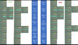
Well, I put this o-scope to use right away (TDS-350) on all the pins of that 239 2122 IC that we've been discussing. I have a video that can better show the pattern of each signal - but for now, I just wanted to give an overview. Hopefully this comes out large enough to be semi-legible (sometimes right-click on the image, copy it, and paste into Paint gives a better view). Each pin of this chip was monitored across both the "GOOD" and "BAD" Display cards, and these images captured for each pin, all using the same x/y resolution (5V and 2.5usec).

Assuming these are IN/OUT pairs of pins, as discussed...

PIN 1 & 2: no real idea what's going on here. PIN1 is repeatable (across both Display cards), but no idea what is the activity going on for PIN 2.

PIN 3 & 4: As expected, PIN 3 is not a sawtooth, but a square wave. This gets echo'd/repeated on PIN 4 for the "BAD" card, but still no idea what PIN 4 is "silent" (0v) on the "GOOD" Card.

PIN 5 & 6: PIN 5 isn't precisely the same across the two cards, but fairly similar. But the main difference is that on the "GOOD" Card, PIN 6 is some kind of wave cycle, whereas on the "BAD" Card PIN6 (Display Request) is a constant 5V - so that's not good. On the "GOOD" card, this Display Request pin is pulled down at some rate, which I assume triggers the actual request-to-display in some fashion?

PIN 7/8/9 are GNDs.

PIN 10 & 11: This is the ALARM activation for the "BAD" card, so no surprise here (where 8.5V is shown on PIN 10). PIN 11 is driving that output. So this being different than the "GOOD" card is not an issue in this case.

PIN 12 & 13: The "BAD" Display card is a bit more "sporadic" on these pins. The "GOOD" Display card seems to "blip" less often to the left side of the scope.

PIN 14 is a Vcc power (5V).


5110Display2392122oscope_summary.jpg


Again, I can provide large views of the above, if needed. But for now looking for just the major deltas in behavior.

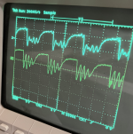
Also, here is C5 (CH2) vs C4 (CH1). In reading this, is it saying the voltage went negative (briefly)?


1656491505816.png
 
Thanks for collecting these traces! This must have taken a while to put together. Congrats on your nice oscilloscope.

I'll get one thing out of the way first and say that C5 and C4 look terrible, and I don't believe in those being good measurements :) I think we'd see failures if the clocks were bouncing around that much. The one thing about them that I do believe is that C5 (the top signal?) comes on a little bit later than C4 does. Is there a chance that you're making poor contact with the probe, or that the ground lead is connected to a poor quality ground?

The outputs on pins 4 and 6 are extremely suspicious to me. Their inputs are similar enough to the "good" card that I'm leaning towards thinking that replacing this IC is probably a step worth taking. Pin 6 alone being stuck high seems like it would interfere with the normal operation of the card and cause problems like the one we're seeing. So far I can't think of a good reason for it to do what it's doing right now: if the input goes low, the output should be low at the same time.

Just for the sake of being exhaustive, can you confirm that there really is no pull-up resistor (or resistor pack) connected anywhere to pins 4 and 6?

Even if there were, pin 6 still should be low when pin 5 is low.

If your measurement is accurate (it can't hurt to double-check), I note that what you're observing here is pretty much @Hugo Holden 's suspicion of "a stuck or defective output line".

As far as pin 12 goes --- I suspect that differences here and other kinds of "sporadic" behaviour may reflect ways that the "rest of the Display Card" behaves when the parts that do handshaking with the computer are acting strangely. That's just a guess though.

To me, the main question is: do you just go ahead and replace this chip now, or do we try and find other defects on this board so that we can fix them all at once? I'd say that if you have a way to replace the part that is likely to be successful, I'd probably just go ahead and do it.
 
I agree on the clock signals, they didn't look at all what I expected them to look like. And I ran out of steam last night to double check and measure other clock points (other cards), will do so soon (and try multiple ground points).
 
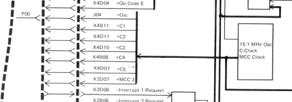
Wait, what's "C4 Pwrd" vs "MCC 4" ? Post #84, I was measuring off the Display card (G2), which has pins J05 ("+C2 Pwrd"), P04 ("+C4 Pwrd"), P07 ("+C5 Pwrd").

Over on the Processor card (J2), it has pin J04 ("+Osc") that looks like the 15.1 MHz clock (it looked like a nice sine wave and the o-scope reported a 15.1 MHz freq). I started probing the X4 and X2 pins mentioned on the SLM for the Processor card - but just touching those pins (with the metal jumper cable) caused the Display to "go funny" so I deemed it too risky until I understood what was going on there better ("X4" and "X2" are like "connector extensions" at the top of the card, I guess to relay additional signals between the Processor and BaseIO cards).

On the Processor card, they are labeled "C1" "C2" "C3" "C4" "C5" (as opposed to "XX Pwrd"). I'm not sure if I can measure C1/C2/C3/C4/C5 on that X4 connector. Following those, they trace over to the BaseIO card. Then they go through a LineDriver and become Powered. e.g. "X4B11 C1" becomes "S02 C1 Powered". Or "X4B08 C4" becomes "S07 C4 Powered". So I'm measuring/monitoring some kind of amplified version of the clock signals? I suppose I won't stress about this, since however they are suppose to be, they appear to be consistent across the two "GOOD" and "BAD" Display cards.

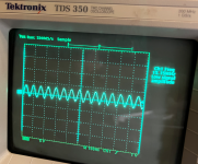
Here is the J04 pin J2 Processor card (labeled as "+Osc"), which if this device is measuring Freq correctly, it matches the expected 15.1 MHz. The thought where the label "CH1" is at on the left side is where 0v is (I guess it is the very bottom of that label that is the 0, so I should raise the signal on the display accordingly). No negative voltage going on here.

1656560788939.png


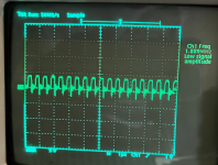
And below, is one of the "+MCC" signals - I forget exactly which one, I think "+MCC 5" (they all look kind of the same for those MCC pins). At least it's a bit more squared.
1656561077717.png
 
Then they go through a LineDriver and become Powered. e.g. "X4B11 C1" becomes "S02 C1 Powered". Or "X4B08 C4" becomes "S07 C4 Powered". So I'm measuring/monitoring some kind of amplified version of the clock signals? I suppose I won't stress about this, since however they are suppose to be, they appear to be consistent across the two "GOOD" and "BAD" Display cards.

It's not so much "amplified", although the concept is similar. You might remember our earlier discussion of "maximum fan-out".

Anything that listens to a signal line also draws a little power from that signal line. Not a lot, just a bit. But if you have enough ICs listening on the line (a big fan-out), then they will draw so much power altogether that the signal's source won't be able to keep up.

You can imagine the extreme opposite: consider that you can set up an arc welder as a nice +20V power supply that can keep on supplying +20V even if you draw a couple hundred amps. Thick cables on the outside and heavy-duty parts on the inside means the welder has no trouble sourcing that current. But as configured, it stays at +20V all the same.

By contrast, the insides of a logic IC are microscopic little traces that only allow a little current to pass from the +5V input to the signal outputs. Too much demand and +5V there slips to +4V, and then lower. If it falls low enough, it can't go above the threshold that distinguishes a 0 from a 1, and even if it doesn't fall quite so far, the signal might not overcome all the other flaws and distances inside the computer. Or, another thing that could happen is that the IC could just try to source all of the current it can through a signal output and fry itself in the process.

The driver IC isn't an amplifier, it's a more powerful signal source that will keep supplying nice +5V signals to many more listeners than the clock generator can support. So it's not amplifying, at least not in the "increases the voltage" sense that we usually associate with an amplifier: it just boosts the amount of current that the signal can supply.

It makes sense for clock signals to have drivers: they will be used everywhere throughout the computer. Lots of ICs everywhere listen to them.

As for Cx vs MCCx, I don't know, but the 5100 MIM has hints:

1656615572828.png

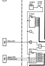
(Ignore -Stop Latch.) C and MCC are separate "clock rings" (batches of phased clock signals), but while C keeps on ticking no matter what, MCC seems to be controllable (presumably started and stopped) by three other signals. (One of them is not shown here.)
 
Last edited:
Neat, there were moment I saw MCC lines with no signal, and I thought I wasn't on the pin properly - maybe it was just one of the conditions that stopped it from ticking.

Recall I said on the X4 (or X2) pins - at the top between the Processor and BaseIO - I said the Display "goes funny" when I touched those with the metal jumper. I didn't get a "screenshot" of that, but to describe it with the GOOD Display installed: the text would "turn to snow" (so fuzzy you couldn't read them), or in some cases a bright vertical line appeared across the center of the screen. And it wouldn't revert when I released the pin - so I quickly released the jumper and mashed RESET. System still seems fine - but if someday anyone is curious about probing pin on those X4/X2 connectors, be cautious, they seem very sensitive to any electrical interference.
 
Very odd. For posterity's sake, do you have a handy photo of the places you tried to probe that triggered that behaviour? (Something to photograph with the computer off, I assume!)

Any thoughts on getting that driver IC on the bad card replaced? :)
 
I can get a shot of the X4 and X2 connectors, yeah not many shots of those pins exposed, so that'd be a good reference. Will do later tonight.

As for the driver IC -- I've contacted a couple shops, but no luck on availability for this kind of work. My plan is to remove the chip, replace in a 14-pin socket, insert the "bad" chip and verify I get the same (bad) behavior. Then I'll mull things over and see how I can verify that the 7412 chips that I have are functional replacements -- a Function Generator has now showed up, so maybe something with that will help (e.g. apply a signal to the IN pins on both, expect to see the same results on the OUT pins {except for the 2 pins that we suspect are bad}).
 
Yeah, it might make sense to wait until you can find a place and a person with the right skill and equipment. If you ask me, this is not a good job for some rando with solder braid and a cheap iron from Home Depot. If you don't see a proper desoldering gun on the bench, then my instinct would be to head for the door :) After all, there's no hurry; you have one working card already.

My one exception so far to the don't-bring-a-Weller-to-a-gunfight rule is Jerry Walker, but he's got a couple hundred videos to earn him the benefit of the doubt.

That said, the important part of this post is: aren't you replacing a chip marked 2392122? That's a 7417 hex driver, not a 7412 3-input NAND. Looks like Digi-Key will sell you a nice new 7417 in a ceramic package for $2; that's maybe bit pricey, but with the confidence I have in their supply chain, I'd feel pretty confident plunking it right into the socket without testing. (Digi-Key lists other 7417 options, but this choice buys directly from them and not their "marketplace".)
 
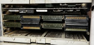
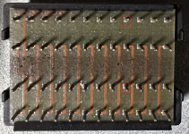
Here is the X4 (left) and X2 (right edge) "connector extensions" that go across the top of the Processor and BaseIO card. They are not interchangeable, so do take care when removing them on which orientation that they were originally (I think they are oriented in opposite directions of each other). Normally a large "rubber stop" runs on top of these pins, so they are not exposed when the A1 board is opened, and act as a kind of brace when the A1 board is closed.


IMG_2851B.jpg

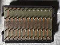
Here is the underside of X2 (the dark spot along the center is from the rubber brace material).

IMG_2848A.jpg


I think both X4 and X2 both use the labels of "B" and "D" for the rows of pins, since those are the only letters used when referencing them. And listed in pin order, (I think) they go like this:


X4B02 NC
X4B03 +Start Execute
X4B04 NC
X4B05 NC
X4B06 NC
X4B07 NC
X4B08 +C4
X4B09 Bus In Bits 7
X4B10 +Bus In Bits 1
X4B11 +C1
X4B12 -Storage Address Bit 0
X4B13 -Storage Address Bit 1

X4D02 NC
X4D03 NC
X4D04 +Op Code E
X4D05 NC
X4D06 +Bus In Bits 4
X4D07 +C5
X4D08 +Gated ROS Select
X4D09 +Bus In Bits 3
X4D10 +C3
X4D11 +C2
X4D12 +Bus In Bits 0
X4D13 +Bus In Bits 2

X2B02 +Program Level Bit 2
X2B03 NC
X2B04 NC
X2B05 NC
X2B06 -Interrupt 2 Request
X2B07 -Control Strobe
X2B08 NC
X2B09 NC
X2B10 NC
X2B11 -Storage Address Bit 2
X2B12 -Storage Address Bit 3
X2B13 +Bus In Bits 6

X2D02 NC
X2D03 NC
X2D04 NC
X2D05 -Interrupt 3 Request
X2D06 -Interrupt 1 Request
X2D07 +MCC3
X2D08 +Select ROS Enable
X2D09 +Program Level Bit 1
X2D10 -Get Strobe
X2D11 -Put Strobe
X2D12 +Bus In Bits P
X2D13 +Bus In Bits 5
 
Then I'll mull things over and see how I can verify that the 7412 chips that I have are functional replacements
There are commercial products but easy to do functional test with Arduino or similar. Little more tricky for devices with internal state/flip flops. Doesn't check speed/drive.

For 7417 open collector driver you will need to add external pullups. Processor may have pullup option on pins but they are normally pretty weak.

See Chip tester on this page for tester I made for checking a PAL. Usage info in comments at the top of code.
http://www.pdp8online.com/TI/ti-portable-professional.shtml
 
These photos are brilliant, thanks!

So just probing some of these X2 and X4 pins causes wonky behaviour? Interesting, I wonder why. None of those pins seem especially sensitive to me.

If I were forced to guess, I'd guess that you were probing one of the clock lines (+C1, +C2, etc.), and the minuscule additional current draw from your probe was enough to reduce the voltage of the clock line below the point where the driver IC could detect it. Knocking out one of the clock phases could cause the computer to do all kinds of strange things.

It still seems odd to me, but it just goes to show that there's always more to learn!
 
Yep, so for example:

X4B08 +C4
X4B11 +C1

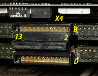
I didn't spot clear documentation about these X4/X2 connectors (though I didn't look in the 5100 MIM), so my assumption (guess) was the arrangement is like this:

1656774713467.png

NOTE: at the bottom left of the connector is some kind of part number (in same material as the traces), It might be B5028202, not 100% sure yet.

The pins at the top, like around pin 4-13, may look like they are "blank" (not connected), but keep in mind their traces are at on the other side.

There are pins beneath the black sections of the connector (like where I labeled "2" and "13"), and if you remove the connector and flip it over, you can verify continuity between the pins as they go across.

Anyhow, yes "touching" what I thought was C4 and C1 caused the bizarre behavior (on the CRT), and I stopped exploring further since I didn't want to possibly damage that CRT. Maybe it's harmless (and maybe I didn't actually find C4 or C1, as I tried several other pins looking for what should be some kind of cyclic pattern). Recall several post back, I did probe "J04" output of the processor that (I think) is the main "+Osc" 15.1Mhz clock, with no apparent impacts to the system (and verified same signal does go over to P06 on the BaseIO card). But true, maybe there are more overall connections on the C1-C5 pins than the "raw" Osc itself - making them more sensitive?

1656776761063.png

We don't know what division each of the clocks uses, right? I mean, they are probably /2 /3 /4 /5 /6, but they don't have to be integer divisions?


ADDITON: for example, the pins marked in the red circle below will have continuity between them (with their trace being on the other side of this small board).

1656777030120.png
 
I didn't spot clear documentation about these X4/X2 connectors (though I didn't look in the 5100 MIM)
I don't think they are described very much in the Logic section of the 5110 MIM. You can find the connections between different diagrams with names like X4D02 and so on, but that seems to be about it --- in that way it doesn't seem too different to the 5110 logic diagrams.

Incidentally, it looks like your pin table is missing some signals. A fair number of the NC pins are the Device Address Bits and Bus Out Bits (5110 System Logic Manual PDF page 5). I discovered this while trying to see if there were any differences between the 5100 X2/X4 connectors and the ones on the 5110. I haven't found any yet, but I didn't look too closely.

We don't know what division each of the clocks uses, right? I mean, they are probably /2 /3 /4 /5 /6, but they don't have to be integer divisions?
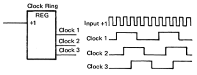
I don't think these are clock divisions in the traditional "clock divider" sense (e.g. 16 MHz, 8 MHz, 4 MHz, 2 MHz, etc.): instead, it's just one frequency derived from the oscillator and shifted into separate phases. You might remember this diagram

1656799086116.png

from this post. It's not uncommon for computers from this time to be driven by multiple clock phases like this, so for a toy example (not the PALM), you could imagine a processor whose first phase (C1) places data into the ALU input registers, C2 triggers the ALU to do an operation, and C3 takes data from the ALU output and places it in its destination.

In fact, using patterns of altered and differently-phased clock signals (especially four of them) was such a common design strategy that there was one computer company that took their name from a related design technique.

PALM uses the phased clock signals in a complicated way that is sort-of described in the MIMs. I say "sort-of" because there are some things that still confuse me about their wording: for example, it sounds like they equate the original 15.1 MHz clock with the MCC, which I just don't think is true. (They also don't mention that there are five phased MCC signals, not just one of them.) Anyway, if you'd like to try to decipher it yourself, you can find text and diagrams at 5110 MIM PDF page 94.


[Random musings about clocking follow.]


Finally, I'll note that the slightly different phase offsets in your "bad" recordings of +C4 and +C5 are pretty easy to see. I can only eyeball it, but it seems like C5 is shifted from C4 by a little more than 60 ns. Given that the oscillator pulses at 66.2 ns, I'm going to guess that this is the size of the shift.

The period of the C4 and C5 pulses themselves seem to be around 650 ns, and I'm going to guess that the true period is 662 ns, yielding a frequency of 1.51 MHz. It's odd to divide a clock by 10, but perhaps that's just IBM's way. On the other hand, your recording of MCC with the Tek scope reports a frequency of around 1.88 MHz, which is a much more reasonable division by 8.
 
Last edited:
Exciting news! A very experienced associate (from the TRS80 CoCo community!) has helped me to put in a 14-pin socket on that one specific IC we've been discussing (the 7417N). Including "period correct" solder (or very near to it).

This 1978 display card is still not fully working, but there is substantial improvement.

Recall the IBM 5110/5100 has a STEP MODE, which you can enable and then step through one instruction at a time. Another special behavior of the IBM 5110 is that on the very first startup cycle, the display card has a special behavior where it queries and display the first 512 bytes of the Executive ROS. (you can then manipulate address lines and exploit this to show any 512-byte portion of Executive ROS, but more on that elsewhere :) ). The point is, on the startup, you have a nice reference display (the Executive ROS in hex format) and not just a random bunch of symbols, so it's consistent on each machine and each startup.


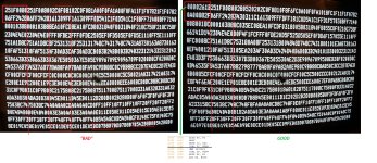
So the good news is, I'm no longer seeing the constant/same symbol across the display. I'm seeing a huge variety of symbols. But when I flip to HEX display - I noticed a pattern (between this "bad" display card and the "good" display card). It alternates "8-bytes bad" (not-matched) then "8-bytes good" (matched).

That's encouraging to me, that the next issue is just some address-pins on another IC chip aren't signaling correctly. I'll look at more pins tomorrow on the oscope.


Below is how the initial REGISTER displays shows up on the "BAD" and GOOD display cards. Recall, the 5110 shows bytes "vertically" - so you can see a full 64-bytes across the display, but its two nibbles are shown vertically (so it takes two rows to show those 64-bytes). I noticed the left side didn't match, but then the right side did. Then I looked closer, and noticed the alternating pattern of not-matching and matching - which was consistent across all the rows.


bad_vs_good_attempt1.jpg


So, not fully there, but one major step forward.
 
Last edited:
Excellent progress! Looks very clearly like address line bit 4 is stuck at logic '1'.

As you say, the hex display doesn't just go left-to-right across the screen, it arranges bytes vertically in stacks of two nibbles (5100 MIM PDF page 152). The fact that each pattern of eight bytes repeats itself means that the addressing that should be counting up like this:

...oooooooo
...ooooooo1
...oooooo1o
...oooooo11
...ooooo1oo
...ooooo1o1
...ooooo11o
...ooooo111
...oooo1ooo
...oooo1oo1
...oooo1o1o

and so on, is instead

...oooo1ooo
...oooo1oo1
...oooo1o1o
...oooo1o11
...oooo11oo
...oooo11o1
...oooo111o
...oooo1111
...oooo1ooo
...oooo1oo1
...oooo1o1o

I'm sure you'll see this on the scope (although the address lines are inverted IIRC, so what you'll see is a stuck +0V). Good luck --- let's hope it's another replaceable part!

PS: What happens if you just let the machine start up normally?
 
Back
Top