• Please review our updated Terms and Rules here

IBM 5110/5100 video Display card repair (possible diode fix)

Where can I find a set of IBM 5100/5110 rom images?

Those are a bit hard to find sometimes. IBM called them "ROS" instead of ROM, so you'd want to search along those lines.

For 5100, I think the best archive is here:
(click SHOW ALL under download options)


I'm not sure why the 5110 ROS's aren't at archive.org, so those are tricky to find also. I include a set in the bin folder of my 5110 emulator, located here
Those come from the following...
The download link there never worked for me from a browser, I had to directly FTP over to
ftp.informatik.uni-stuttgart.de/pub/cm/ibm/ibm5110
Thank you very much!
 
Have you checked pin 1 of the LS157 chips for proper activity? That is what selects which input signal goes to the output of the chip.

I masked off all the other pins around PIN 1 of each of the 74157 chip. The results were consistent on both the "BAD" and GOOD Display card. Which is:

IC1 and IC2 were mostly 5V, but had sporadic brief pull down to 0V. I didn't have an extra hand to image while holding the probe, but essentially like this:
1658603967821.png

IC1 = 1582601 / 767396 ==> 74157 (DATA SEL/MUX)
IC2 = 1582601 / 767396 ==> 74157 (DATA SEL/MUX)

IC10 and IC11, as far as I could tell, stayed at 0V always.

IC10= 1582601 / 767396 ==> 74157 (DATA SEL/MUX) flat 0V in STEP and RUN
IC11= 1582601 / 767396 ==> 74157 (DATA SEL/MUX) flat 0V in STEP and RUN


Assuming that's all OK, it's a bit of a puzzle. Just for fun, could you measure the resistance to ground on the 7492B's pin 6 and compare it with some of the other signal input pins to that chip, pins 1-5, 7, and 9?

(assume meant 74298?)

74298 pin resistance comparison on IBM 5110 Display Card (pin 8 is ground in this chip, but I kept the probe on the A1 connector pins D08 GND just as a more stable point to latch onto).

Code:
         "BAD"       // "GOOD"
 1-8 ==> 20.5  Mohm  // OL
 2-8 ==> 22    Mohm  // OL
 3-8 ==> 1.290 Kohm  // 1.230 Kohm
 4-8 ==> 1.290 Kohm  // 1.240 Kohm
 5-8 ==> OL          // OL
 6-8 ==> 0.735 Mohm  // OL
 7-8 ==> 1.290 Kohm  // 1.240 Kohm
 8-8 gnd
 9-8 ==> 1.290 Kohm  // 1.240 Kohm
10-8 ==> 30    Mohm  // 23    Mohm
11-8 ==> OL          // OL
12-8 ==> OL          // OL
13-8 ==> OL          // OL
14-8 ==> OL          // OL
15-8 ==> OL          // OL
16-8 ==> 0.566 Kohm  // 0.459 Kohm


20+ Mohm is essentially the same as OL?

pin 6 is an obvious outlier here. But it's not obvious how this difference translates to the issue we're seeing.

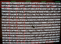
Recap - that issue is, the BAD display is repeating its content every 8th column (across each row). I'm still trying to rationalize how that's happening. Assuming the RWS content is correct, the Display is showing content that contradicts the 0x200 - 0x600 RWS region it should be latched to.
1658605195542.png

So... if I assume the COL/ROW counters are working ok... Say at the top left, COL 0, ROW 0. That corresponds to some address:
0x200, 0x201, 0x202, 0x203, 0x204, 0x205, 0x206, 0x207 ... (first 8 chars)
0x208, 0x209, 0x20A, 0x20B, 0x20C, 0x20D, 0x20E, 0x20F ... (next 8 chars)

As @stepleton mentioned earlier, from this appears the "4th bit" is stuck "on". So where the Display think it is drawing address 0x200, it is querying RWS 0x208 and drawing that content instead. When the Display gets to drawing 0x208, it ends up querying the correct RWS 0x208 address (again).

1000000000
1000000001
1000000010
1000000011
1000000100
1000000101
1000000110
1000000111

1000001000 (next 8 chars)
....

BusOut has a PARITY bit line also. I assume because of this "stuck bit" the Display is saying the BusOut content doesn't jive with the Parity value, and induces the RED InProgress light (which I thought would cause a RESET or freeze/system halt, but instead just seems to be corrupting part of the Display - maybe just the Display is resetting and the CRT content appears partial {in RUN mode}, but the system at a whole seems to be completing the ROS checks and Language ROS startup).

So..... Bus Out could be used by H2 (BaseIO) to tell the Display which address to query? (but this is 0-255, so it's some offset from some base address - I don't quite understand the Device Address X vs Y pins. to speculate:

0x200 00 (first 4 rows of 256)
0x300 01 (second 4 rows of 256)
0x400 10 (third 4 rows of 256)
0x500 11 (fourth 4 rows of 256) (0x5FF end of display buffer)
BO DA.X ?

As this P11, pin 6 of 74298 is a "4th index" (BO-3), maybe it is the cause of this issue we're seeing?


(and did blast most of a full can of compressed air - same result though)
 
Also, I've ordered a couple copies of each of these DIP chips, just to have them available. Except one of them I couldn't find:
IC5 = 2396261 / 721153 ==> 1231 (COUNTER)

(except one on eBay, and a little expensive compared to the others -- and then not sure if it was exactly the same chip or not, so I'll keep looking around -- but at the moment, I don't think I'm having any issue with the counter chips)
 
pin 6 is an obvious outlier here. But it's not obvious how this difference translates to the issue we're seeing.
Thanks for taking these measurements. It could actually be relevant to the fact that the P11 signal can only rise to +2V.

On the healthy card, there's a lot of resistance between Pin 6 of the 74298 (not 7429B, thanks!) and ground. On the sick card, it's 735 Kohm. 735K is a pretty high value for a resistor, but it's a lot smaller than a few dozen megaohms. The source of the P11 signal can only pump so much current into P11: if there is a low enough resistance path to ground on that pin, then the source simply won't be strong enough to overcome that drain and achieve a full +5V.

Unfortunately... I'd expect the outputs of most ICs to be strong enough to overpower a 735K resistor and raise the logic line to +5V. If V = IR, then I = V/R = 5/735000 = about 7 microamps. That's not a lot of current.

It would be lovely if we could say "hey, the chip got a little fried and now there's an obvious low-impedance path to ground on pin 6" but it's not so simple. It may be that this path only opens up when the Display Card has power.

What this does tell us is that some Display Card I/C on P11 is bad (which we suspected) and that the problem is not likely due to some debris on the circuit board (otherwise I'd expect a much lower resistance than the 735K you're seeing). A chip DID get a little fried, I think, just in a more complicated way.


At this point it's not too clear what to do to diagnose things further. Maybe some other electronics-savvy folks out there know better than me. About the only corrective action you can do at this point anyway is to replace the 74298 chip and pray that this is where the fault was. If the problem is in the metal can ICs, then there's not a lot we can do about it.

BusOut has a PARITY bit line also. I assume because of this "stuck bit" the Display is saying the BusOut content doesn't jive with the Parity value, and induces the RED InProgress light (which I thought would cause a RESET or freeze/system halt, but instead just seems to be corrupting part of the Display - maybe just the Display is resetting and the CRT content appears partial {in RUN mode}, but the system at a whole seems to be completing the ROS checks and Language ROS startup).

I think you're on to something here, but I'm starting to wonder if there are TWO separate problems at work.

First, here's this from PDF page 113 of the 5110 MIM:

1658612304362.png

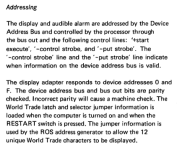
I think the Display Card has several jobs. One of those jobs is to be the place where the 5110 does parity checking on the Bus Out and Device Address Bus lines. This check has to be somewhere in the machine, and IBM decided to put it into the display card.

This parity checking doesn't really have much to do with the display. I think your display problem is a separate issue.

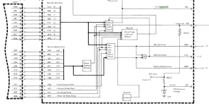
Take a look at the System Logic Manual diagram (PDF page 6) for the display card parts that use Bus Out:

1658613461890.png

Complicated! And check it out, there's "Bus Out and DA Parity Check" right in the middle.

But notice that despite all the inputs and all the outputs, there are only two skinny little signals that go up to the other part of the diagram, up where all of the display stuff happens. One of them is the "World Trade Latch and Selector", which (according to the paragraph I copied above) doesn't seem too related to the problems we're dealing with --- it seems to be about modifying the character set or something. The other thing is the -I/O Display Off signal, and I think in this case, it's just the mechanism by which the processor can enable/disable the display (through I/O writes to device 0). It looks like a parity check fault can do the same thing.

In other words, there's nothing in this section that can cause the video problem we're seeing. That means the Bus Out bits aren't related to the display problem. It's a second, separate fault. One of these chips is dragging down P11, which probably causes a Bus Out parity error, which causes a PROCESS CHECK.

So..... Bus Out could be used by H2 (BaseIO) to tell the Display which address to query?

I don't think so. There's not much that I/O writes can do to the display: it can turn it on or off (writes to device 0), it can do some weird "World Trade" thing which I don't know about but don't think is relevant (also device 0), and finally it can reset the display adapter (writes to device F).

I predict that if you replace the 74298 chip and it fixes the P11 sag:
- the display problem will remain
- the PROCESS CHECK problem will go away

If replacing the 74298 chip doesn't fix the problem, you might consider removing the Machine Check jumper (5110 MIM PDF page 186) so that the PROCESS CHECK problem stops bothering you and you can keep troubleshooting the display problem (which will be somewhere else).


That said, I would still be anxious about the fact that the P11 line can't go above +2V. The P11 source probably is getting stressed trying to raise it to +5V and failing, and this could cause it damage in the long term. I'm not sure what the right thing to do about that is.
 
"World Trade" I guess is their fancy way of saying "internationalization character support." And in another thread (here) I cycle through all those jumpers to see what the character set looked like -- mostly just adjustments to accents on vowels and currency symbol changes. The paragraph you mentioned explicitly calls out copying (to somewhere) the 12 modified symbols (there are about 15 total "character sets", each one just has 12 modified symbols from some baseline set).


But you're right, I forgot to elaborate that there are two apparent issues: (1) the 8-character blocks of repeated symbols (which only appear static when the machine in STEP mode), and (2) when in RUN mode, the symbols are essentially not-legible , where it appears to me you just get 1 or 2 rows of the character set (kind of dots spread across the screen, but since I know what the normal bootup should look like - I can also see a few extra dots where that normal text would appear -- the "ABCDEFGHJKLMN" at the top and the ERR 013 D080 content at the bottom).

Example: the below looks like "garbage" while in RUN mode. But in STEP mode, we get fully formed characters (and blank spaces)
1658649900670.png

On the Commodore PET, there was this "hack" that someone found where you could just write the top pixels of a character, then do some kind of interrupt and start the drawing again -- this gave an impression of having actual graphics on the PETs' normally text screen. That's the general gist, it may have been much more elaborate than that. Point being, maybe a similar effect is happening here - a few pixel rows of the characters are getting drawn. Then some kind of RESET happens (from the Parity fault?). In our case, it gives the effect of just 1 or 2 rows of pixels being drawn on the screen.
 
Last edited:
Point being, maybe a similar effect is happening here - a few pixel rows of the characters are getting drawn. Then some kind of RESET happens (from the Parity fault?). In our case, it gives the effect of just 1 or 2 rows of pixels being drawn on the screen.

I think something like this could be possible.

Note that I/O instructions talking to Device F can reset various systems inside the 5110. Since the Display Card is corrupting the Bus Out bits, it's possible that an ordinary I/O instruction is being interpreted by the Display Card as a reset signal.

Of course, the P11 line isn't +2V for just the Display Card --- the fault is causing the voltage on this Bus Out line to sag across the entire system. So perhaps some other card is getting confused and resetting everything.

But when things are broken like this, it's hard to be certain what's wrong. We'll just have to keep collecting evidence and making theories, and hopefully we'll learn more as time goes on.
 
I think the Display Card has several jobs. One of those jobs is to be the place where the 5110 does parity checking on the Bus Out and Device Address Bus lines. This check has to be somewhere in the machine, and IBM decided to put it into the display card.

In the IBM 5110 SLM System Logic Manual SY31-0552-3_405-03 it has a poster for Process Check. On the bottom of that, I noticed this chart:

1658680436160.png


So it seems each device has its own "local" bus out parity check?
 
@Hugo Holden got some numbers on the older CRT used in the 1978 IBM 5110 (possibly more like one also used in the 5100):
GTE Sylvania CRT
type 5ST6111A
part no. 1-014-0716
CODE 2-739

EDIT: there is another small number on the sticker, hard to make out but think it reads E1A312

Would they make both the CRT and the PCB attached to it? Looks like Sylvania still exists - but more automotive lighting related stuff. And looks like Sylvania was involved some legal battles vs Continental Television regarding franchise licensing and the Sherman Act, heavy stuff related to some foundational philosophy of anti-trust, competition, macroeconomics. Whew, when you just wanna sell Widget A (CRTs) and it balloons into some national debate. Then again, CRTs relate to precision beam-steering, I suppose derived from radar-tech. So, kind of sensitive stuff in terms of what markets should have access to it?
 
Last edited:
So it seems each device has its own "local" bus out parity check?

You know, I was about to say "probably not", but checking the logic diagram:
- the Base I/O board has parity checking
- the Common and Language ROS board has parity checking
- the Parallel I/O board has it

and indeed the diagram on the System Logic Manual page where you'd snapped that image clearly shows multiple cards all doing the same parity checks. Huh. I wonder why on earth all of this redundancy was necessary.

The MIM talks about running the machine with various cards removed, I think (for diagnostic purposes), so maybe this redundancy was to give you a good chance of having the circuitry in place to raise a Machine Check even if you didn't have a full set of boards.

Looks like Sylvania still exists

Sylvania used to be a major electronics manufacturer: they made light bulbs, radios, vacuum tubes, semiconductors, and even computers at one point. I think it's likely they had their fingers in so many pies that antitrust problems were probably inevitable. Can you share photos of this Sylvania-powered VDU?
 
Hey all, I'm having trouble finding this IC:

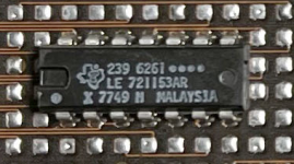
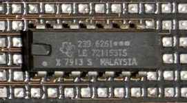
IC5 = 2396261 / 721153 ==> should be "1231" (COUNTER)

I see a 16-pin version (here), but I think I need a 14-pin version.

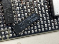
Here's the best shots I have on file from two different cards.

1667378877204.png 1667378890775.png


Suggestions on a 1231 source or suitable substituted appreciated, thanks!


I've found sources for all the other IC DIP on this display card, this is the last one I'm looking for.
 
The LA1231 IC you found is an FM radio IC, and not related.

Most 14 pin logic IC's are usually gates, and the simple versions of the counters

The best move is to scope its pins (on the good board at least) and find out its logic function.It might give a clue as to the correct part number.

One tiny clue that I can see is that pin 2 & 3 are connected together, so it cannot be one of the more common common two input AND, NAND or NOR gate, like the 08,09,00,26,32,37,38, and some others. It could be a simple hex buffer, or a FF or a counter. Some typical counters in the 14 pin package are the 90, 92 & 93.

Check which other pins are connected will help with the puzzle,along with thes cope tests.
 
Last edited:
The bottom of that chip says "X23184HAH" or maybe "X23184HAN". I have an IC tester that tests/identifies the usual 74 series logic and that tester could not find a match. It also does not check for 74184 but that IC has 16 pins so I think that one is ruled out.

I've fixed a display board without replacing that IC (because I didn't know what it was to test) but I did replace other 74 series logic. Maybe try to fix it without touching that one. I also have another display board that is not fixed but I need to fix this one too. At this point, I figured it might be one of the big chips on this one.

IBM5100-displaychip.JPG
 
If the gates are NAND or NOR connecting the inputs together makes the gate work as an Inverter.
But, this IC , cannot be a common NAND or NOR, because if you connect pin 2 and 3 together, you would be connecting a gate's output, to the same gates input. Most of the common AND, NAND, NOR have pins 1 & 2 as an input and pin 3 as an output, so you don't see pin 2 & 3 connected on these gates. Though you might on a common Hex inverter, or hex buffer IC or some flip flop & counter IC's, or gates that have more than 2 inputs.

To find out what this IC is requires checking with a scope, at least 4 channels probably, to determine its logic function. The numbers are not giving much of a clue.

The first move in determining what sort of TTL IC this is , is to determine which are its power supply pins by checking the pcbs.

You don't want to be caught out, because the IC needs to be powered in a test setup for analysis.

Most, but not all 14 pin TTL IC's have the gnd on pin 7 and the plus supply on pin 14...but, some do not.

This was described perhaps in more polite words than a blunder, in Horowitz & Hill's book, the Art of Electronics.

For example, look up the common garden 7490 and 7493 counter IC's: the gnd pin is on pin 10 and the +5V on pin 5, yes that is right.

This is why the pcb needs to be inspected.

Once the power supply pins are determined, the IC can be set up in a test jig, it is then easy to determine which of the IC's pins are inputs, which are outputs and which are N/C. Because of the current sourced & sunk by the pins. Then once that is known it significantly narrows down the possibilities of what the IC could be.

(as an aside, I liked the line in the Clint Eastwood movie, the Eiger Sanction. He had caught a bad guy and said to him "Who sent you ?" the man replied "My Superiors" and Clint said; "that narrows it down" )

PS, Just some TTL trivia that you would never win a prize for unless you were on a cruise boat, doing a quiz for retired electronics engineers who grew up with TTL's: They fixed up the "stuff up" with the 7493 and the 7490 counter power supply pins, later on in the history of TTL IC's, by making replacements for them, what were they ? Answer; the 74LS390 and 74LS393, that had the supply pins back to pin 7 gnd and pin 14 +5v.
 
Last edited:
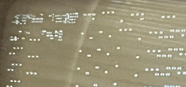
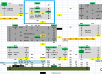
Here's the notes I have when exploring the pins of that chip from awhile back (the area in the blue square).

This was turning the board over, looking down on the "pad" side (so the pins are "reserved" from "normal"). Between each IC is a two space gap of additional pads and tracing/connections.

As mentioned, most IC on this board, pin 7 is ground, and the last pin (14) is power.

But this "239 6261" chip is different (what I call "the 5th chip" in along the top) - continuity with ground is at pin 10, and continuity with power is on pin 5.

Aside from pin 10, I may not have finished tracing pins 8-14 (there are no annotations there -- either I didn't find any, or had run out of time then).

But pins 2 goes to S13 (on connect at bottom right, no shown in this diagram) and pin 7 goes to J10 (on the connector below this chip on this diagram). I'll try to find my other notes to get clarification on what those two pins are. I thought I had a nice diagram about all those, but I'm not finding it right now (might be on another PC). Actually it might be earlier in this thread, will check a little later.


1667610189747.png
 
Confirmed, pin 2 and pin 3 are connected to each other on this "1231" IC.

Some notes I have say S13 should be GND, and I confirmed those two pins do have continuity with S13. But S13 doesn't seem to really be connected to the other GND pins on this same board. This effectively means pin2 and pin3 are Not Connected (since J13 doesn't seem to go to anywhere else in the system).

Pin 7 (J10) is also simply "not connected."

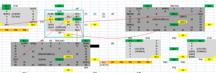
I still haven't resolved pin 4, 6, and 13. But I did find leads to the other pins, as follows: (we don't know what the silver "tincan" do - but we did find a replacement to that IC04 and should know what it does). (T) (P) (Z) (Y) (X) are just my accounting of here-to-there, they don't mean anything.

1667623422679.png


And incidentally, we've socketed all these IC's I've replaced all the other ones. This display card no longer causes the speaker to BEEP or the red in progress light to stay illuminated, but now nothing is showing up on the CRT at all.
 
But this "239 6261" chip is different (what I call "the 5th chip" in along the top) - continuity with ground is at pin 10, and continuity with power is on pin 5.
Probably it is a 7490 or a 7493A, possibly a 7492A but not a 74L92 (because that oddball variation has the Vcc on pin 4 !)

To find out, you need to check the IC in operation on the board, or the IC placed in a test jig & look at the clock pulses, or feed them in and test the flip flop outputs. Very often the the 7490 or the 7493, has the Q output of the first flip flop pin 12, connected to the B input of the second flip flop pin 1 so check if they are connected on the pcb.

The '90 counter had more internal gating compared to the '92A and 93A. The truth tables are in the Texas Instruments TTL data book, or online as pdf's.
 
Back
Top