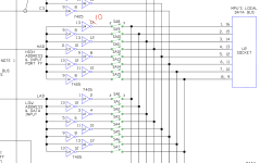
working through the verifying switch functions and connections per the 2014 schematic on the CP-A. All looking good except SW8 is connected to U4 7405 pin 10, not pin 12 as in the schematic. pin 12 is not used as best I can tell. does this make any sense? possibility of an error in this re-made schematic?
- VCF South West - June 14 - 16, Davidson-Gundy Alumni Center at University of Texas at Dallas
- VCF West - Aug 2 - 3, Computer History Museum, Mountain View, CA
- VCF Midwest - Sept 7 - 8 2024, Schaumburg, IL
- VCF SoCal - Mid February 2025, Location TBD, Southern CA
- VCF East - April 2025, Infoage Museum, Wall NJ
-
Please review our updated Terms and Rules here
You are using an out of date browser. It may not display this or other websites correctly.
You should upgrade or use an alternative browser.
You should upgrade or use an alternative browser.
IMSAI newbie, no idea what I'm looking at
- Thread starter Dokken
- Start date
daver2
10k Member
Yes, there appears to be errors on this schematic...
U4 pin 12 IS used though, it is used by the switch associated with SA7.
I have a way of testing the gates, switches and wiring out if you want to do that next (using your logic probe).
Perhaps I will post that for you tomorrow if you are interested...
Dave
U4 pin 12 IS used though, it is used by the switch associated with SA7.
I have a way of testing the gates, switches and wiring out if you want to do that next (using your logic probe).
Perhaps I will post that for you tomorrow if you are interested...
Dave
you are of course correct about pin 12...
I've checked switch resistance, all are at 2-3 ohms, pretty comfortable with those.
front panel is installed after testing, cleaning switches and same status with the stuck led.
yes, please send me the test info!!!
I've checked switch resistance, all are at 2-3 ohms, pretty comfortable with those.
front panel is installed after testing, cleaning switches and same status with the stuck led.
yes, please send me the test info!!!
Last edited:
daver2
10k Member
Ok, if you look at the schematics for the front panel you should notice that all of the 7405 gates (including the address/data switches) are divided into four (4) groups driven by the signals LAD, HAD, C3 and NOOP.
The four groups are connected to a common bus going to socket U2.
A 7405 gate is an open collector inverter. As such, they do not have a pull-up to 5V. The pulls-up resistors are all on the CPU board (after U2).
First thing, after a power-up, STOP and RESET; can you measure the state of signals LAD, HAD, C3 and NOOP using your logic probe.
They should all be LOW with no pulses on them.
A LOW input to the 7405 gates should make the outputs all float. If all of the address/data switches are CLOSED, your logic probe should read all HIGH signals on socket U2.
That is the first test.
Let me know what you obtain.
Dave
Thank you.
Partial results below, I'll have to do some creative gymnastics to get the results on pins 1-7 as they're not accessible due to the switches. I'll get to that next if needed.
only cards installed are CP-A and CPU. press Stop, reset.
pin 8-14 in order
U1 LHLHLHL ok?
U3 LHLHLHL ok?
U4 xLLHLHL
U6 xLLHLHL
U7 LHLHLHL ok?
x on U4 and U6 is no probe signal
daver2
10k Member
First off, what are the states of the four individual logic signals LAD, HAD, C3 and NOOP after a STOP followed by RESET?
Dave
Dave
daver2
10k Member
Excellent.
So all of these signals LOW means that we are feeing a LOW into all of the 7405 inverters and (therefore) the output from all of the 7405 inverters should all be open circuit.
With all of the address/data switches CLOSED - this should mean that the signals on the U2 connector should all be HIGH (due to the action of the pull-up resistors on the CPU card).
Also, with all of the address/data switches CLOSED, the outputs from all of the 7405 inverter gates should also be HIGH (due to the action of the pull-up resistors on the CPU card 'feeding back' through the CLOSED address/data switches). In addition, the outputs from the 7405 inverters that do not go via a switch should also be HIGH.
Is this all correct?
Dave
daver2
10k Member
I also forgot to say, any HIGH that should be present on connector U2 should also result in the associated DATA BUS LED bit to be ILLUMINATED.
This might be an easier way to 'see' the logic level on U2. It also tests the 74LS04 inverters and the LEDs on the data bus indicators...
Dave
This might be an easier way to 'see' the logic level on U2. It also tests the 74LS04 inverters and the LEDs on the data bus indicators...
Dave
daver2
10k Member
Just looking back at your previous posts, I suspect U4 pin 8 being 'X' to be associated with your address line bit 9 (SA9) fault.
Follow the PCB track from U4 pin 8 looking for bad solder joints and broken PCB tracks etc.
Do the same for U6 pin 8.
You definitely should not have an 'X' - only a HIGH or LOW (assuming the switches are truly closed/made).
Dave
Follow the PCB track from U4 pin 8 looking for bad solder joints and broken PCB tracks etc.
Do the same for U6 pin 8.
You definitely should not have an 'X' - only a HIGH or LOW (assuming the switches are truly closed/made).
Dave
disregard everything in post 25 above. I had the chip orientation off due to lack of coffee this morning, pins 1-7 of the chips are visible above the switches from the front. I'll recheck that now.
I did pull the cp-a and re-flow most chip socket solder. nothing obvious, but I'll re-check as above.
I did pull the cp-a and re-flow most chip socket solder. nothing obvious, but I'll re-check as above.
Last edited:
daver2
10k Member
I have pressed the ERASE button on my brain ") !
!
Dave
!Dave
My brain still only has a rubout button. old school.I have pressed the ERASE button on my brain
Dave
daver2
10k Member
The same!I don't have to press "erase". My brain does it for me. I often sit down to look something up on Google or DuckDuckGo and within 5 seconds can't remember what it was. I hate when that happens.
Dave
ok, re-do of the 7405 U 1, 3, 4, 6, 7 tests. stop, reset, no ram. only pins 1-7 are readily accessible without some work.
starting at pin 1 going through 7
U1 LHLHLHL
U3 LHLHLHL
U4 xLLHLHL
U6 xLLHLHL
U7 LHLHLHL
I don't immediately see U4 or U6 pins 1/2 on the schematic.
what next?
starting at pin 1 going through 7
U1 LHLHLHL
U3 LHLHLHL
U4 xLLHLHL
U6 xLLHLHL
U7 LHLHLHL
I don't immediately see U4 or U6 pins 1/2 on the schematic.
what next?
daver2
10k Member
>>> I don't immediately see U4 or U6 pins 1/2 on the schematic.
Neither do I.
You should be able to find the points required on one end of SA0-SA7 or one end of SA8-SA15.
U2 (on the CPA) is also wired to 9 (on the CPU board) which is wired to the data bus pins of the 8080 CPU - if that is of anymore help.
Dave
Neither do I.
You should be able to find the points required on one end of SA0-SA7 or one end of SA8-SA15.
U2 (on the CPA) is also wired to 9 (on the CPU board) which is wired to the data bus pins of the 8080 CPU - if that is of anymore help.
Dave
daver2
10k Member
So is everything in posts #28 and #29 as we expect?
Dave
Dave