Chuck(G)
25k Member
Also, you might get more bang for the buck by substituting the 80C188EB processor. Lots of nice stuff there and readily available. The 80C188EC is even better, but you don't get it in PLCC--it's available only in 100-pin QFP.
We have already gone through the same comments with the OP in a separate thread regarding the choice of CPU.Also, you might get more bang for the buck by substituting the 80C188EB processor. Lots of nice stuff there and readily available. The 80C188EC is even better, but you don't get it in PLCC--it's available only in 100-pin QFP.
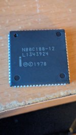
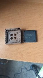
I already have a PLCC-68 80C188. It's just the standard version, which is what I want to use. I'll upgrade to the better versions in the future of this projectAlso, you might get more bang for the buck by substituting the 80C188EB processor. Lots of nice stuff there and readily available. The 80C188EC is even better, but you don't get it in PLCC--it's available only in 100-pin QFP.
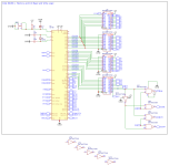
I was told that for a small 80188 computer, I don't need to use the bus transceivers for the Data Bus. The datasheet for the CPU shows a typical computer setup diagram of which I'll show in this reply.
I'll just say this. I'm not trolling. This is a new hobby for me and there is still a lot for me to learn about building a computer like this. I apologize for my unprofessional behavior. I know what I want to build stemming off of this prototype. I was just paranoid about the parts that glue this project together, the Logic Chips. I'll fix the pin headers for the Data Bus in the next board design that'll be based on the new advice given to me in this post.Okay, it’s a “small 80188 computer”, I‘d agree with that… until you started bellyaching about how you needed all this massive drive strength for the address lines because of the bazillions of peripherals you were going to add to it. (That you’re setting the threshold for “bazillions“ comically low is another matter.) Which is it, is this a “small computer” or not? If your handwave for this is you can just add a data bus transceiver later, here’s my responses:
A: you’ve already broken a general design guide no-no by running that unbuffered segment through an external connector; even if you tack a bus transceiver onto your expansions you’ve put a source of potential noise on the wrong side of it.
B: you need some logic to set the direction/enable for this part, it makes way more sense to build that now and get it over with, integrated onboard, and,
C: if this is your attitude, that it’s a small computer and if signal integrity is something you’ll worry about later, then why wouldn’t you also just say ”eh, I can always slap a line of ‘244s on my card if I need to reset address bus fanout” instead of wasting all this ink asking about what Hercules strength parts to use for your apparently *intentionally* half-baked bus now?
This is why I’m kind of wondering about that trolling theory. At the very least it seems like every discussion about this thing turns into schizoid ping-ponging between whether the goal you’re building towards is a desktop computer or a wall-size MultiBus monster, and at random you seem to completely conflate the requirements for the former with the latter… except where you don’t and decide you’re building an embedded SBC.
I'll fix the pin headers for the Data Bus in the next board design that'll be based on the new advice given to me in this post.
4 layer boards aren't too expensive nowadays, but 6+ layers are considerably more. Also with 4 layers you have a reasonable chance that mistakes can be fixed with a cut and strap.


If I was this uncertain about an unproven design, I wouldn't start with PCB. I'm old-school--I'd do a wire-wrap version first.

Do you envision any external devices will do bus-master DMA transfers?I only have one minor concern. The Bus Transceiver (U18) that's used for the Memory doesn't have logic for the OE, so I just put it to GND. Is that a problem?
Not really.Do you envision any external devices will do bus-master DMA transfers?
I only have one minor concern. The Bus Transceiver (U18) that's used for the Memory doesn't have logic for the OE, so I just put it to GND. Is that a problem?
I knew it! Thank you so so much!Yeah, that’s not really great. A better idea would be to AND together all the chip selects that are behind it so it’s only enabled when one of them is. Otherwise this is going to drive the bus and ruin your day if you interface a memory device to your expansion bus.