• Please review our updated Terms and Rules here

Original-IBM-5150 or IBM-Clone Memory Experimentation Thread

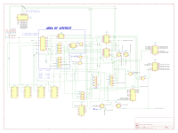
Okay, looking closer at the memory datasheet and this page, I found that the timing for the RAS-CAS-WE cycle seems to be within the proper range of at least 200ns.

Still, I'm still confused, and we're back to square one as to why the data disappears. (Which is probably what is causing address 0001 to fail)

I couldn't read the Refresh Gate with my logic analyzer, for some reason, even though I seem to have found it in my own schematic. I may figure that out later in the day tomorrow.
 
Last edited:
Okay, this keeps getting weirder and weirder...

On a hunch, I modified your code, @modem7, to read from address 0002. (I've worked with extremely simplistic formatting before, so I know endianess and binary flags and all that.) I got a trigger on the logic analyzer! It didn't do that with the address 0001 ROM!

I want to try modifying it again to try writing and reading from address 0003. If I don't get a trigger then, there's something up with the way the system is wired.
 
AHA! We may have a "checkerboard" problem! That is, every odd-numbered/second address is either not getting the data, or the data is being erased! (My money is on the memory chips not getting the data at all)

Addresses 0000 and 0002 work, but 0001 and 0003 do not! I didn't get a trigger when I tested the latter!

Screen Shot 2023-09-15 at 2.38.04 PM.png

Looking over my schematic, I found that I hadn't connected these pins to anything. It's odd, because one of the halves of U81 is responsible for driving RAS0 and RAS1, and pins 2 and 13 on U67 are on that same Address Strobe line, same as U81. So, if for the sake of argument, why isn't pin 5 and pin 10 on that same connection? (I'm not saying it needs to be, just odd that only half the chip is being used.)

I'll take a look with my multimeter and see where those unconnected pins go.
 
U81B has to do with Parity. (Pin 5 is the DATA-OUT pin for the parity chip.)

U81C goes off to a 245. I'm not sure what that has to do with anything.

Still stuck. At least we know there's a problem with the addressing, somehow.
 
To my mind a “checkerboard” pattern with every Nth cell working/not working could mean an issue with address multiplexing. Do you have traces that cover accessing several addresses and verifying that A0-A8 actually increment appropriately? Depending on how the RAS/CAS generation is muddled up with the address decoding you could also be suffering a case where bank select isn’t correct (the read/write cycle is going to the wrong bank), or you’re only getting an active cycle on certain bit patterns because that part of the circuit is still thinking banks are 64K instead of 256K. A clean schematics without question marks of what the actual state of the circuitry is would help a lot.
 
Do you have traces that cover accessing several addresses and verifying that A0-A8 actually increment appropriately?
I think I may understand now:
  • A0-A8, as binary switches translated into hex, provide the place/address of a specific value within the chip.
  • RAS and CAS signals the chip to either accept input, or send an output.
  • WRITE-EN actually allows the chip to accept the input.
What you want me to do is check if the CPU's addressing circuitry is able to set A0-A8 correctly, so that the output place is the same as when it set the input place.

For example, if we say a value is in "001011010", even if one binary switch is wrong and we get "000011000" (Yes, it's two wrong, but say there's more than one problem with the addressing), we're not going to find the value that we want, and the system will either throw an error, or not continue entirely.

EDIT: Oooh! It's just a thought, but maybe that's why 256k mode can set A0-A7 to correct addresses, but 640k mode cannot, because of that extra A8 value! (i.e. all the odd addresses use the LSB of 1 in their values! The other even-numbered address values don't!)
 
Last edited:
I think I may understand now:
  • A0-A8, as binary switches translated into hex, provide the place/address of a specific value within the chip.
  • RAS and CAS signals the chip to either accept input, or send an output.
  • WRITE-EN actually allows the chip to accept the input.

When the DRAM chip sees /RAS (row address strobe), it writes (address write, not data write) the row address specified by address pins A0-A8 into the chip's row-selection circuitry.
When the DRAM chip sees /CAS (column address strobe), it writes (address write, not data write) the column address specified by address pins A0-A8 into the chip's column-selection circuitry.
So, /RAS, /CAS, A0-A8, are about selecting a particular cell in the chip. See [here].

/WE at HIGH = Read mode. Read the selected cell's contents and present that to the Dout pin.
/WE at LOW = Write mode. Write the state of the Din pin to the selected cell.
 
Okay, I may have a basic idea of what is wrong, according to VOGONS. It's the A0 line, providing the "1" portion of the address (i.e. A1="2", A2="4", etc), as opposed to A8. I'll take a look at it in a bit.
 
Well, what do you know?

I'm very tired, but I think I did this correctly. I swear there were no continuity beeps from my multimeter when testing.pins unconnected?.pngpins unconnected? 2.png

See U25 and U26 up there? Half of their output/input pins are not connected, according to my continuity tests. They are part of the addressing system. I can test again tomorrow, but, oof.


If I didn't know better, I'd say that seems to stick out like a sore thumb.
 
I am unsure what you are doing. Are you doing continuity testing on your Sanyo motherboard, based on the circuit diagram of a different motherboard ?
 
I am using the 5160's schematics as a basis for my Sanyo, and changing the pin assignments on the schematic to match. So far everything, including logic chips, matches up. (Even now.)
 
Last edited:
I am using the 5160's schematics as a basis for my Sanyo, and changing the pin assignments on the schematic to match. So far everything, including logic chips, matches up. (Even now.)
I wonder if, like the IBM 5160, the Sanyo motherboard has a ROM for address-to-RAM-bank decoding.

You can see that ROM (U44) in the diagram at [here]. To the left of the ROM is jumper pad E2, and a jumper is put on 1-2 as part of the process of upgrading from 256K MAX mode to 640 MAX mode. The jumper selects a different part of the ROM to be used, i.e. effecting different address-to-RAM-bank decoding.
 
According to a member of the Tech Tangents Discord, there's a set of chips that already serve that purpose, which I had highlighted "AREA OF INTEREST" in the schematic. The JP6/J6 jumper changes the setup, without having to use a ROM.

I'll take a close look at the RAMADDRSEL explanation that you added, though. That might help me.

I've included an updated version of the schematic:
 

Attachments

  • Schematic Update.png
    Schematic Update.png
    877.5 KB · Views: 4
You really need to stop it with the 5160 schematics. This is a different computer. Yes, it uses largely the same parts to do the same job, but those parts can be connected in a practically infinite combination of ways to do it. You *need* an accurate understanding of how *your machine* is put together if you hope to modify it.

I mean, flatly speaking the fact that this machine doesn’t use a PROM for address decoding makes it more like a 5150 than a 5160; I think I pointed out earlier how the later version of the 5150 motherboard modified for 64Kbit DRAMs has appendix-like leftovers of the circuitry for using 16K chips on it, I would strongly suspect that’s a better analogy for what’s happening on this board relative its unimplemented/incomplete 640K support.
 
I know this is different from the 5160, but it's as close as it will ever be to one. The MBC-775's documentation is also laughably rare-to-nil. (I've looked. Believe me, I've tried.) I'm still waiting for an appropriate time to send off another request for a 775 manual scan (which may or may not have schematics of its own) from a museum, which is in the middle of an article move at the moment and won't be ready until 2024. The 5160's original schematics are all I have, looking for differences and similarities between the two. It's difficult enough trying to trace the circuit from-scratch. It's as best as I can get.

So far, I'm seeing many similarities to the 5160, slowly gaining an understanding about how the memory in this system works, and how its circuitry is analogous to the 5160.
 
Last edited:
Well, at the very least, in both modes, a full address is being correctly expressed in the proper timing according to the address lines on the chips, and those values are inverted, like you said, modem7. (i.e. FE instead of 01 and FC instead of 03)

I will try to correlate it with the data-ins and -outs.
 
I was too tired to remember if this was part of the trace, earlier this morning:
If we are reading from Addr 0001, we should have the inverted value of 01FE in 640k Mode, correct? (not counting the leading 0 as part of the value. The reason is my logic analyzer does that too, so the value comes out as 3 numbers, which fits in with the idea of the LS138's operation)

If so, then the addressing seems fine.

Also, I did more editing of your ROM, modem, and I found something interesting: Not only do just the even addresses report correct values, but there's not just a checkerboard pattern of good address/bad address/good address, etc. either.

There is a sub-checkerboard pattern in the odd addresses, according to the PC analyzer card I got in a few days ago.
Every alternate odd address is either 00 or FF.

Here's how it goes:
0001: 00 (Bad)
0002: Good
0003: FF (Bad)
0004: Good
0005: 00 (Bad)
0006: Good
0007: FF (Bad)
0008: Good

I saw the values change between address 0001 and 0003 and thought I had modified them wrong. It seems not, and there was something else involved.
 
Last edited:
I've been tracing out the circuitry more and more, and finding more analogous structures.

Unfortunately, I'm having a bit of trouble trying to figure out where to start from now:

For the sake of argument:
1. Timing for Row and Column Address Strobing (RAS/CAS) and Write Enable all seem fine.
2. Addressing seems fine, if my logic analyzer is to be believed.

The actual problems:
1. The memory affected is all odd address numbers. Even address numbers seem fine, and the analyzer card reports perfect reading.
2. The odd addresses alternate with values of 00/FF/00/FF...

I modified your code again, modem, so it would read and write 55 and AA values to addresses 0000-0007, but using two individual ICs for respective even and odd addresses, just to make sure that the memory writings were consistent. (As you can see, the last two odd addresses would report 00 and FF, as you as coded in your version, but they were just a fluke and not actually the "read" values.)
 
Last edited:
You can further develop the circuit diagram on an as-needed basis.

How about this:

You could modify the code to write/read only one of the failing addresses, i.e. 00001
And write/read only one value, a value that you know, at address 00001, returns a different value to that written.
Then, pick one RAM chip in bank 0 that corresponds to a bit that does not read back as expected.
Then in with the logic analyser (LA).

Step 1:

Assumption: LA is good enough for the task.

Via the LA, verify that all inputs to the RAM chip are expected: levels and timing. If not as expected, go back through the circuitry to work out what is wrong. Otherwise, on to step 2.

Step 2:

All inputs good. Does the LA show the expected bit coming out of the RAM chip during the read phase ?

If no, lift the data pin out of the socket, and see if the bit is still not as expected. If still not as expected, then things do not make sense: Compatible and known-good chip; output pin isolated and so cannot be affected by load; but bad data bit out for good inputs !!!

If yes, then the problem is either:
- The bit (good) is 'damaged' somewhere on its way from the RAM chip to the CPU; or
- The CPU is getting the bit okay, but there is a problem from CPU to POST card.

To prove the former, modify the test code, e.g.
Write value XYZ.
Read back value.
If value read back is XYZ, then do {action 1}.
Otherwise do {action 2}.

{Action 1} and {Action 2} should not involve the parallel/LPT POST card (we want to 'eliminate it from the equation'). So, {action 1} could be something like toggling a particular pin on the 8255, and {action 2} could be toggling a different pin on the 8255. Similar to what TEST6082 and TEST6083 at [here] do.
 
... the analyzer card reports ...
Presumably the parallel/LPT type. The ISA POST cards are questionable on XT-class computers.

Note that when modifying test code for the parallel/LPT type:
- Ensure there is an adequate delay between bytes sent to the device (otherwise the device doesn't see some bytes).
- Ensure that the possibility of duplicate bytes are not sent. E.g. If sent is {99], delay, {99}, then the device will only register one of the {99}.
 
Back
Top