• Please review our updated Terms and Rules here

Original-IBM-5150 or IBM-Clone Memory Experimentation Thread

Done. It is TEST5060 at [here].

Note: In the capture, the address shows as FF instead of 00. That is because, on the IBM 5150 motherboard, the address gets inverted on its way to the RAM chips.

Note: Because dynamic RAM refreshing has not been initialised, there should not be any /RAS or /CAS activity on banks other than bank 0.
 
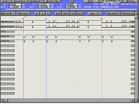
All right, I'm not sure how much use this is going to be. All the information (To the best of my interpretation) and timebase are there. I even put in some markers just to make sure, and give you a time reference.

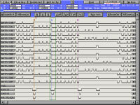
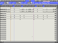
Read-Write of 55h:
55h RW.png

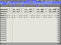
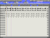
Read-Write of AAh? (S is in the same area, but not on the falling edge after the memory is zeroed out. I think I moved that marker by accident.)
AAh RW.png
 
Before I comment of the captures, some points/recaps follow. Sometimes a revisit helps.

* The motherboard works in 256K MAX mode, but fails in 640K MAX mode.

* You are unaware of anyone getting 640K MAX mode to work.
Therefore the possibilites are:
- On your motherboard, '640K MAX mode' is a work-in-progress (possibly finished in later motherboard revisions).
- On your motherboard, a faulty chip.

* 256K MAX mode
Bank 0 : 64 Kbit chips, Address range 0 - 64 KB, /RAS and /CAS must only go to this bank for the bank 0 address range.
Bank 1 : 64 Kbit chips, Address range 64 - 128 KB, /RAS and /CAS must only go to this bank for the bank 1 address range.
Bank 2 : 64 Kbit chips, Address range 128 - 192 KB, /RAS and /CAS must only go to this bank for the bank 2 address range.
Bank 3 : 64 Kbit chips, Address range 192 - 256 KB, /RAS and /CAS must only go to this bank for the bank 3 address range.

* 640K MAX mode
The bank you have labelled as connected to CAS0 : 256 Kbit chips, Address range 0 - 256 KB, /RAS and /CAS must only go to this bank for the bank 0 address range.
The bank you have labelled as connected to CAS1 : 256 Kbit chips, Address range 256 - 512 KB, /RAS and /CAS must only go to this bank for the bank 1 address range.
The bank you have labelled as connected to CAS2 : 64 Kbit chips, Address range 512 - 576 KB, /RAS and /CAS must only go to this bank for the bank 2 address range.
The bank you have labelled as connected to CAS3 : 64 Kbit chips, Address range 576 - 640 KB, /RAS and /CAS must only go to this bank for the bank 3 address range.

* In 640K MAX mode, you have the 256 Kbit chips in the banks that you have labelled as connected to CAS0 and CAS1.

* Ruud's Diagnostic ROM shows a data error at address 0.
 
Last edited:
Your version of Ruud's diagnostics shows a failure on the very first address that it reads: 0000 (I forget the format, but the point is that the diags reports a failure in memory right out of the gate, at address zero.)
Out of curiosity:
1. A version of 3.6 or later ?
2. What bits are indicated in error ?
3. Any change if the chips in banks 1, 2 and 3 are removed, or did you already do that ?
 
Out of curiosity:
1. A version of 3.6 or later ?
2. What bits are indicated in error ?
3. Any change if the chips in banks 1, 2 and 3 are removed, or did you already do that ?

1. Yes. I tested with v3.6.
2. All of them. Taking out the LS139 to affect a change did seemingly cause one. (I believe it was bits 0, 1, 3, and 5 that were considered bad in that case.)
3. I already took out all the memory in banks 2, 3, and 4. (Only bank 1 is populated.)

Before I comment of the captures, some points/recaps follow. Sometimes a revisit helps.

* The motherboard works in 256K MAX mode, but fails in 640K MAX mode.

* You are unaware of anyone getting 640K MAX mode to work.
Therefore the possibilites are:
- On your motherboard, '640K MAX mode' is a work-in-progress (possibly finished in later motherboard revisions).
- On your motherboard, a faulty chip.
Correct. I'm not too worried about adding or removing wires. My system has quite a few bodge wires already from the factory.

* 256K MAX mode
Bank 0 : 64 Kbit chips, Address range 0 - 64 KB, /RAS and /CAS must only go to this bank for the bank 0 address range.
Bank 1 : 64 Kbit chips, Address range 64 - 128 KB, /RAS and /CAS must only go to this bank for the bank 1 address range.
Bank 2 : 64 Kbit chips, Address range 128 - 192 KB, /RAS and /CAS must only go to this bank for the bank 2 address range.
Bank 3 : 64 Kbit chips, Address range 192 - 256 KB, /RAS and /CAS must only go to this bank for the bank 3 address range.

* 640K MAX mode
The bank you have labelled as connected to CAS0 : 256 Kbit chips, Address range 0 - 256 KB, /RAS and /CAS must only go to this bank for the bank 0 address range.
The bank you have labelled as connected to CAS1 : 256 Kbit chips, Address range 256 - 512 KB, /RAS and /CAS must only go to this bank for the bank 1 address range.
The bank you have labelled as connected to CAS2 : 64 Kbit chips, Address range 512 - 576 KB, /RAS and /CAS must only go to this bank for the bank 2 address range.
The bank you have labelled as connected to CAS3 : 64 Kbit chips, Address range 576 - 640 KB, /RAS and /CAS must only go to this bank for the bank 3 address range.

* In 640K MAX mode, you have the 256 Kbit chips in the banks that you have labelled as connected to CAS0 and CAS1.

* Ruud's Diagnostic ROM shows a data error at address 0.
All correct.

Majenko from the Tech Tangents Discord gave me a basic rundown that everything already exists to allow 640k. (Same person who helped TT figure out the ISA card for his rare 5150/60/70-era CD-ROM drive.)

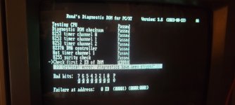
With all chips in place (including the LS139), for the Ruud Diag, it shows 0000:0001 as the location of the error, with ALL bits bad. Same with the Supersoft Diags.
 
Last edited:
2. All of them. Taking out the LS139 to affect a change did seemingly cause one. (I believe it was bits 0, 1, 3, and 5 that were considered bad in that case.)
If that LS139 drives a data bus, then you would have ended up with an un-driven data bus. Some people think, "Well then, an un-driven bus will be either all one's or all zeroes (depending on design)." but in practice, things can be different.

Your version of Ruud's diagnostics shows a failure on the very first address that it reads: 0000 (I forget the format, but the point is that the diags reports a failure in memory right out of the gate, at address zero.)
With all chips in place (including the LS139), for the Ruud Diag, it shows 0000:0001 as the location of the error, with ALL bits bad. Same with the Supersoft Diags.
00001 (0000:0001 in a segment-offset format) is the second RAM address, not the first.

Confirm 00001.
 
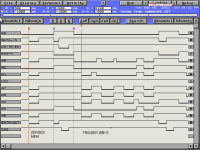
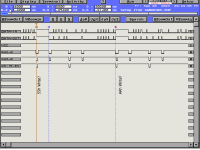
All right, I did another sampling. Took me a while to connect all the test points.

I'm assuming the pulses before the Trigger "T" is the zeroing of the memory?
Sanyo MEM Reading.png

Now this is peculiar. There are missing pulses in DATA-OUT.
Mem reading missing pulses.png

Also, 00001 confirmed.
20230906_001530.jpg
 
Confirm 00001.
Okay. You have confirmed it. That is odd. Let me have a think about that.

( Depending on my research, it might be that I will modify the code-for-ROM to write/read address 00001 rather than 00000. )

I'm assuming the pulses before the Trigger "T" is the zeroing of the memory?
At no stage does my test code zero any RAM. It does not need to be zeroed.

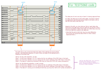
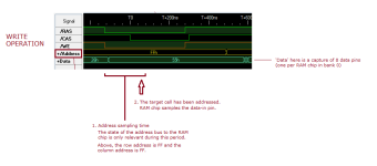
For a write operation:
Step 1: The address of the target cell is fed to the RAM chip via a row address followed by a column address. See the fictional example at [here].
Step 2: After a short delay, the chip writes the state of the data-in pin into the target cell.

Per the diagram in post #146, the state of the address bus into the RAM chip is irrelevant outside of the RAS/CAS period.
And the state of the data-in pin is irrelevant except for the very short time of step 2 above.

Do not worry about anything outside of the RAS/CAS period.

Now this is peculiar. There are missing pulses in DATA-OUT.
Sometimes, one needs to expand in on only the areas of interest:

1693984216330.png
 
00001 (0000:0001 in a segment-offset format) is the second RAM address, not the first.
Okay. You have confirmed it. That is odd. Let me have a think about that.

( Depending on my research, it might be that I will modify the code-for-ROM to write/read address 00001 rather than 00000. )
I cannot see a bug in Ruud's Diagnostic ROM.
Indications are that, on your computer, address 00000 passed, and then failed on address 00001.
Interesting.

I will shortly DM to you a variation of TEST5060, one that writes/reads address 00001 rather than 00000.

Perhaps use it first with your motherboard set to 256K MAX mode, so that you know what to expect using your logic analyser.
 
And looking at your captures, I suspect that on each RAM chip (perhaps except for the parity ones), the data-out and data-pin is connected together.
(I.e. if so, no need to capture both pins separately.)
 
When I tested the connection between DATA-IN and DATA-OUT, they didn't seem to be connected, so that's why I captured both pins.

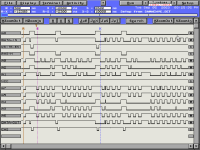
This is the capture with the latest version of the code you sent to me, in 640k mode:

ANA Test 1.png

And a wider view of the capture:

ANA Test 3 (256K MAX).png

And a wider view in 256k mode.

ANA Test 2.png
 
When I tested the connection between DATA-IN and DATA-OUT, they didn't seem to be connected
I thought that you would have been more sure than "seem". It should be a case of, pick a RAM chip in bank 0, except for the parity chip. On that chip (still in socket), measure the resistance between the data-in and data-out pins. If less than, say, one ohm, then the pins are connected.

This is the capture with the latest version of the code you sent to me, in 640k mode:
You can clearly see a write, then a read, then a write, then a read, etc.
But what is needed is two things:

1. The capture to include the data pins of each bank 0 chip (except for parity). That way you can see what bytes are going in and out. I don't need to see that. You need to be satisfied that what is read back is what was written in.

2. The RAS, CAS, and WE signals are present, but what cannot be clearly seen is the relationship between those three signals. Zooming in on the various 'RAS/CAS are asserted' areas is required, like what I showed in post #151. Then compare that to the timing in 256K MAX mode (i.e. the mode that works).

Re point 2 above. I am not expecting you to see a difference. You have a board that works in 256K MAX mode but not in 640K MAX mode.
In going between those two modes, the engineer would be catering for two things:
1. The RAS and CAS going to different banks depending on bank size.
2. In 640K MAX mode, two banks have 256Kbit chips rather than 64Kbit chips. How to deal with the extra address pin on the chips.
It doesn't make sense that the design would change the RAS/CAS/WE timing between the two modes.
 
All right, I've taken a look. I think I might be getting the hang of the basics.

My multimeter does not show that the data pins between in and out are substantially connected; it reads 4 megaohms.

I also found a way to expand the data bus (instead of outputting 1 when the hex value is detected)

In 256k mode:
1. It's complicated, but Data-In and Data-Out looks the same as the Read-Write-Cycle diagrams in the memory I'm using (NEC D41256C)
2. The binary values on each 8-bit data bus (in and out) seem to match what MacOS' programmer calculator shows me. (i.e. 01010101 for 55h, and 10101010 for AAh)

In 640k mode:
Same. HOWEVER...

I believe I have found our culprit!

In 256k mode, if I am reading this correctly,

The memory value 55h is written (Cursor R, WRITE_EN is low), and is correctly read (When RAS and CAS are asserted the second time at Cursor X)
Same when it's written with AAh when written (Cursor S), and when read.
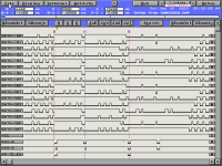
ANA Test Final (256K Mode).png

But in 640k mode...

ANA Test Final (640K Mode).png
WHERE'S MY DATA?! (Highlighted in Green, at Cursor X)

Value 55h is missing when RAS and CAS are asserted!

Another problem that may have arisen, CAS seems to have shifted! (It doesn't start halfway through RAS assertion, or terminate at its rising edge, which is what the data sheet says its supposed to do!)

Strangely, Value AAh seems to be fine, as you can see after Cursor S on the second capture.
 
Last edited:
I just checked the 640k mode sample I took last night, to make sure it wasn't a one-time fluke at the start of the sample. It isn't. It seems every alternate read, that is, when it read-writes 55h, doesn't correctly report the value of 55h back, and it's ONLY on the reading of value 55h!

256k mode seems to keep the value. And also, even 256k mode's CAS timing doesn't line up perfectly. At the very least, it seems to be asserted correctly.
 
Last edited:
And also, even 256k mode's CAS timing doesn't line up perfectly.
When I look at your capture screen shots, I see a measurement problem. If I am interpreting your software's output correctly, then your logic analyser is only sampling at 5 MHz. That is, the state of each line is sampled every 200 ns.

To get the kind of timing resolution shown below, I have my logic analyser sampling set at 100 MHz (10 ns).

1694387921023.png
 
Even at a higher sampling rate (I just now tried at 25 MHz), value 55h is completely gone in 640k mode when RAS and CAS are asserted for a read, and CAS does not terminate on the rising edge of RAS and WRITE-ENABLE.
 
Last edited:
Even at a higher sampling rate (I just now tried at 25 MHz) ...
I am guessing that is as high as your analyser allows.

... and CAS does not terminate on the rising edge of RAS and WRITE-ENABLE.
The timing diagrams in the datasheet of the NEC µPD41256 show a certain amount of leeway.

Or are you indicating that you seeing different RAS/CAS/WE timing between 256K MAX and 640K MAX mode ?

On the subject, the µPD41256's are something else unique to the 640K MAX mode. Proven good elsewhere? I guess that at some point, you swapped into bank 0, the second set of µPD41256's.
 
Back
Top