• Please review our updated Terms and Rules here

Original-IBM-5150 or IBM-Clone Memory Experimentation Thread

And returning to my mind is that, in 640K MAX mode, Rudd's Diagnostic ROM is passing the data test of address 00000 and then failing on 00001 (showing all bits in error).
In 640K MAX mode, if you remove a data chip from bank 0, does Rudd's Diagnostic ROM then fail the data test at address 00000 ?
 
I am guessing that is as high as your analyser allows.
My analyz(s)er (lol) goes up to 50MHz. Even then the 55h value disappears when RAS and CAS are asserted for a read in 640k mode.
Or are you indicating that you seeing different RAS/CAS/WE timing between 256K MAX and 640K MAX mode ?
I am seeing different RAS/CAS/WE timing. 640k mode doesn't match the Read-Write Cycle diagram in the datasheet. 256k mode does, almost exactly. Maybe there is leeway in it, but all I know is that the timing has shifted, as you can see in post #156.

Proven good elsewhere?
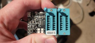
I do have a RAM tester (4164/41256 on the right), and all of them tested as good. I can try testing again, though.
20230911_014706.jpg
 
And returning to my mind is that, in 640K MAX mode, Rudd's Diagnostic ROM is passing the data test of address 00000 and then failing on 00001 (showing all bits in error).
In 640K MAX mode, if you remove a data chip from bank 0, does Rudd's Diagnostic ROM then fail the data test at address 00000 ?
Good call. Yes, it does.
To me that is weird. Not a problem at address 00000, but a problem at address 00001. Surely the RAS/CAS/WE timing is the same for both.

I know you have a parallel/LPT reader device. Within minutes, I will DM to you a couple of BIN files. One does test write/reads of address 00000, and the other of address 00001. It will be interesting to see what the CPU is reading back.
 
I do have a RAM tester (4164/41256 on the right), and all of them tested as good. I can try testing again, though.
You have at least two sets of 41256, one intended for bank 0 and one intended for bank 1.
You will have tried both sets in bank 0 (I presume).
The odds would be very very low that both sets contain a chip that is faulty at the second address.
 
I actually have a lot of 41256 memory chips, because I wanted to upgrade my Macintosh 128k as well. Swapping around the chips to test was partly what initiated reaching out to VCFed, because I wasn't sure if there was a problem with how my system read the chips, or if the chips themselves were faulty.

Unfortunately, I don't have an LPT reader device, but it shouldn't be difficult to build one. I have a modern ISA POST Card, but that's it.

If it will work the exact same way, I can read the logic coming from the LPT port with my analyzer.
 
Unfortunately, I don't have an LPT reader device, but it shouldn't be difficult to build one. I have a modern ISA POST Card, but that's it.

If it will work the exact same way, I can read the logic coming from the LPT port with my analyzer.
Still, acquiring one of the readers is a good idea. Very cheap, and saves time.
 
To me that is weird. Not a problem at address 00000, but a problem at address 00001. Surely the RAS/CAS/WE timing is the same for both.
You have at least two sets of 41256, one intended for bank 0 and one intended for bank 1.
You will have tried both sets in bank 0 (I presume).
The odds would be very very low that both sets contain a chip that is faulty at the second address.
I wrote "second address", which is true for the 'motherboard' address, but different for the address that reaches RAM bank 0.
That is because your capture in post #142 shows that like for the IBM 5150 motherboard, the address gets inverted on its way to the RAM chips - the row is FF and the column is FF (not 00 and 00).

( And in some motherboards, the motherboard-address-to-row-column circuitry does something else - it 'scrambles the address lines about. )

If you use test code that targets only motherboard address 00001, I wonder what the row and column addresses become.
 
All right, I was able to get some info, just with my logic analyzer. (I sent off for one of the LPT diagnostic readers on eBay, though.)

In 640k mode, and sampling at 50MHz, the logic analyzer triggers at all reads through the LPT port with the Address 0000 test IC. However, it does not trigger with the Address 0001 test IC. Strangely, I kept getting triggers for 00h with the 0001 test IC, but the appearance of the readings were not consistent with the appearance from address 0000 (just a scramble of pulses, rather than the number, then the memory read), so I think it's safe to assume that it was not working either.

In fact, I was able to get almost the exact same appearance in post #158 on my analyzer's readings. (with the hex number appearing and the crossed pulse waves)
 
In 640k mode, and sampling at 50MHz, the logic analyzer triggers at all reads through the LPT port with the Address 0000 test IC. However, it does not trigger with the Address 0001 test IC. Strangely, I kept getting triggers for 00h with the 0001 test IC, but the appearance of the readings were not consistent with the appearance from address 0000 (just a scramble of pulses, rather than the number, then the memory read), so I think it's safe to assume that it was not working either.
Just to confirm:

The expected bytes out of the LPT port, in a continuous loop are:

1. Write 55 to address. Small delay. Output [01] to LPT followed by [byte read back from address].
2. Two second delay.
3. Write AA to address. Small delay. Output [02] to LPT followed by [byte read back from address].
4. Two second delay.
5. Write 00 to address. Small delay. Output [03] to LPT followed by [byte read back from address].
6. Two second delay.
7. Write FF to address. Small delay. Output [04] to LPT followed by [byte read back from address].
8. Two second delay.
9. Loop back to 1.

Because we have no idea what is going to be read back from the address, the byte triggers used would be 01/02/03/04.
 
With the Address 0001 IC, the analyzer didn't detect any triggers.
Very weird.
So no additional info provided by that code-for-rom.

In 640K MAX mode, a write-then-read of address 00000 works, but not of address 00001.
Of course, the address is changing between those two states.

But is anything else changing? With your logic analyser not set to 50 MHz sampling, do you see any difference in the RAS/CAS/WE timing? With this motherboard, it's becoming a case of 'expect the unexpected'. As I see it, you really have to dive in deep with your logic analyser.
 
Yes, like I said, there is still a difference in RAS/CAS/WE timing. CAS seems to assert and terminate earlier than 256k mode (256k's mode being pretty much the textbook example of timing, according to the datasheet), just like post #156 shows. I'll sleep on it (literally) and take a good look at the 640k sample that I got when I figured out how to interpret the pulses, just to make sure that WE's seeming bad timing in that post was not a fluke.

I'm reminded of a similar premise with a ZX Spectrum having a similar memory timing problem being repaired with a capacitor. Right now, I'm a bit tired, so I can't remember exactly what video I found it in, in this YouTube member's video list: https://www.youtube.com/@JoulesperCoulomb/videos
 
No. There is no difference in timing between addresses in 640k mode. The only thing that changes the timing is if the 256/640k jumper is installed. (Again, it's textbook perfect in 256k mode, but changes in 640k mode.)

EDIT: I found the video I was talking about, with the capacitor in the ZX Spectrum, starting at 4:42:
 
Last edited:
Sorry, I meant that separately between addresses in either mode, there is no change in timing. The only change that occurs is the overall RAS/CAS/WE timing when switched-between using the 256k/640k jumper.
 
Last edited:
EDIT: I found the video I was talking about, with the capacitor in the ZX Spectrum, starting at 4:42:
From what I heard in that video, the RAS-CAS delay is achieved via a resistor and capacitor, rather than a delay line, and a capacitor was added elsewhere to effect a small delay.
From a work-in-progress circuit diagram of your motherboard that you posted earlier, I see a delay line.

No. There is no difference in timing between addresses in 640k mode. The only thing that changes the timing is if the 256/640k jumper is installed. (Again, it's textbook perfect in 256k mode, but changes in 640k mode.)
Sorry, I meant that separately between addresses in either mode, there is no change in timing. The only change that occurs is the overall RAS/CAS/WE timing when switched-between using the 256k/640k jumper.
If I look at what IBM does in an upgrade of an IBM XT motherboard from 256K MAX to 640K MAX, I see:
1. Changing which bank RAS and CAS goes to depending on the motherboard address; and
2. Adding a 74LS158 chip to cater for the extra RAM address pin, A8.
3. Fitting 41256 class chips into banks 0 and 1.

I do not see IBM adjust the RAS/CAS/WE timing in the move to 640K MAX configuration.

BTW. In the work-in-progress circuit diagram of your board, I see that the equivalent to the 74LS158 chip above, is the chip that is labelled as 'U45 74158 (EXTRA)'.

So as I see it, a question is, does the circuit diagram indicate that the observed different RAS/CAS/WE timing is expected in 640K MAX configuration ?
If the answer is no, use the circuit diagram to hunt down the faulty component/s causing the timing change.
If the answer is yes (and the timing observed is as the circuit diagram indicates it should be), is the timing suitable for the fitted RAM chips.
 
Taking a look at both circuit diagrams, at a quick glance, it suggests that the CAS length is set too short, but I cannot be sure.

If the delay line affects the CAS length or when it happens, it is supposed to be set for a 100 ns delay according to the original schematics, if we can use that as a standard. My computer's is set for 20ns, at the very least.

On mine, the CAS is generated by similar chips to the 5160, with a few extras in-between, but both the original 5160 and my clone always start with a delay connected to an (L)S00, which is then connected to a 138, which generates the CAS signal.

I'm not sure if I'm grasping at straws here, but that makes the most sense, given the change in timing.
 
Last edited:
Okay, never mind. I'm probably wrong. Another Turbo XT motherboard manual shows the same delays already connected on my system.
 
All right... it's probably obvious at this point, but I just wanted to reiterate the problem.

What we seem to be dealing with is:
  1. the normal operation of data being written. The data is able to be read back out in 256k MAX mode. This is its basic operation.
  2. that same operation being done in 640k MAX mode, but the data is completely gone. Either it's been erased, or it's not refreshed properly or fast enough.
I'm going to go out on a limb and say another path we should take is looking at the refresh circuitry. Is this being done externally by the system, or is it provided by the chip?

Then again, there's the oddity of it affecting Address 0001, not 0000.

EDIT: Maybe it's not CAS and WRITE_EN being affected, but RAS and its refresh. I have to do more research, but a quick glance at diagrams in the 5160 manual and my diagram, and your page here, modem, shows that there's some kind of relationship. Again, I'm going out on a limb, so it may seem like I'm grasping at straws.
 
Last edited:
Back
Top