• Please review our updated Terms and Rules here

PDP-12 #435 at the University of Minnesota Duluth

I think you should go back to the oscilloscope to understand what the signals really look like.

What is the sample rate you're using for the Saleae?
Good idea. Looks like the sample rate is 500MS/s, and Saleae says the maximum digital bandwidth is 100Mhz. I guess I'm not sure what rate that NOR clock will run at. We should be able to use the 'scope on Monday. Thanks!
 
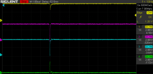
Hi, @antiquekid3 -- we used the scope today to look at the NOR clock in C16 that generates LC 02. Our scope does 500Ms/s with four probes in use.
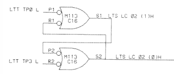
1726515851256.png

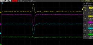
Yellow - C16 S1 LTS LC 02 (1) H
Pink - C16 R2 LTT TP3 L
Blue - C16 P1 LTT TP0 L
Green - C16 S2 LC 02 (0) H

Here's what it looks like running @ZachyCatGames 's code; notice the yellow, pink, and blue pulses, which are pretty tall, and the green pulses, which are quite short.
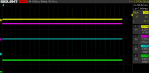
1726512924224.png

Zooming in one one of those clock ticks, we see:
1726512980378.png

Thinking that maybe the short green signal is a marginal signal from one of the ICs, we found yet another M113 to swap in (this time, from A26). When we run the test with this other M113, we get a signal that we think looks a lot better -- nice spikes on all four channels:
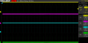
1726513191609.png

Again zooming in on one "tick":
1726513213623.png

Does that look right to you? We notice that, in the latter images, yellow (S1) switches from default low to default high (i.e., yellow is high and "dips" instead of being low with "raises"). I was thinking this might be because (in the latter images) S2 is actually working correctly.

In this state, the machine seemed to generate the Tape Word FF signal pretty consistently. (We could not confirm that it was exactly right, and we didn't try running Mark 12, becuase the A24 M113 we borrowed was also tape related.)

Next, we ran the FC tester on the M113s that were not generating the S2 signal correctly, but both M113s passed the tester in multiple runs. Zach also tried changing the test delays but that did not seem to affect anything.

One super weird thing happened when we were working with the FCT. When we plugged one of the M113s into the tester, the UUT power light would come on dimly, even when the power was switched off. (The UUT power light would light up to its normal brightness when we switched the power on.) Is this indicative of anything? We confirmed this happening a few times, but then it stopped happening before I could get pictures and we haven't been able to replicate it since. (@vrs42 have you seen this happen before?)

This was all so weird that we will probably try to recreate everything again tomorrow or Wednesday to make sure that we aren't crazy.

We wondered if we should maybe try scoping the S2 pin while the FCT is running to see if we are getting weak signals from the S2 pin. How do we do that?

Finally, if the M113s are actually putting out good signals on the S2 pins, is the next thing to look at the flip chip slot itself? Can I spray deoxit straight into the FC slot? Or what is the right method for cleaning slots? Since we are probing directly from the pins all on the same slot, I wouldn't think that it is a wire wrap issue.

Sincerely,

Dumbfounded in Duluth
 
When looking at narrow pulses, be sure to capture the pulses with the timebase set accordingly, rather than zooming in after a triggered event. You're going to lose a lot of resolution that way.

1000027360.png

1000027361.png

1000027362.png

Time to start looking at B38 and C18, I believe.
 
D'oh. Looking back at the code, bits 6 and 7 do not need to be set at the same time. Everything on the 'scope looks pretty normal with that taken into account.
 
@antiquekid3 -- thanks for the tips on the scope... I am still learning.

I'm alarmed by the inconsistency of our results... @ZachyCatGames and I will rerun some of these tests until we get something consistent.

Do you happen to know if we can spray deoxit straight into a flip chip slot, and if so, if we have to wait a particular amount of time before powering on the machine? My understanding is that it is non-conductive but I'd prefer confirmation on that point. :)

Or, if deoxiting the slot isn't the way to do it, what is the recommended way to clean a flip chip slot?

Thanks again for everything!
 
I'm alarmed by the inconsistency of our results... @ZachyCatGames and I will rerun some of these tests until we get something consistent.
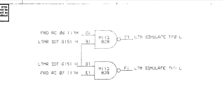
The reason for the behavior is you're asking the flip-flop to set and reset at the same time, given you are issuing TP0 and TP3 simultaneously—hence, the non-deterministic behavior.

Deoxit is fine for the slots. Some prefer spraying it on cardboard and then inserting that in and out of the slot. This could create fiber shreds, but I haven't heard an issue with that.

From the symptoms so far, I'm not seeing any signs of backplane issues.
 
The reason for the behavior is you're asking the flip-flop to set and reset at the same time, given you are issuing TP0 and TP3 simultaneously—hence, the non-deterministic behavior.
ohh, yeah that explains a lot. We spent awhile trying to figure out what it was supposed to do if TP0 & TP3 were triggered at the same and were getting very confused lol.

I updated my program to generate TP0 and TP3 using separate instructions. I now get a nice buzz from the speaker. Though running it slowly in single step mode seems to show TWC is still not always skipping (edit: I looks like it's consistently skipping every 4 attempts).
Code:
4020    1020    LDA I       // Set AC bit 4 so IOT 6152 clear tape word FF
4021    0200
4022    0500    IOB
4023    6152    IOT 6152
4024    0437    TWC I       // Really make sure tape word FF is clear
4025    6024    JMP 4024
4026    1020    LDA I       // Set AC bit 6 so IOT 6151 generates TT0
4027    0060
4030    0500    IOB
4031    6151    IOT 6151
4032    0301    ROR 1       // Rotate AC right by one so bit 7 is set
4033    0500    IOB         // so IOT 6151 generates TT3
4034    6151    IOT 6151
4035    0417    TWC         // Check if tape word FF is set
4036    6020    JMP 4020
4037    0011    CLR         // clear, set, and clear AC to make a speaker click
4040    0017    COM
4041    0011    CLR
4042    6020    JMP 4020
 
Sounds like this was a red herring. I'd recommend trying MARK12 again and trying to look at the problem again, if you're sure it's still passing the tape controller diagnostics.
 
Sounds like this was a red herring. I'd recommend trying MARK12 again and trying to look at the problem again, if you're sure it's still passing the tape controller diagnostics.
That's what I was thinking, too. We can scope the tape word flip flop and maybe even C16's M113 when it's waiting for the twff and see what we see.
 
1726766006053.png

Well, we ran Mark 12 and scoped LTS LC 02 (0) H (the signal leaving the NOR gadget), LTS LC 01 (1), LTS LC 00 (1), and the output of the Tape Word Flip Flop (not shown). Nothing happens. (Recall that when we run @ZachyCatGames 's TP0 / TP3 exerciser, we get a nice signal).

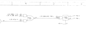
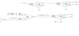
This got us thinking that maybe the "simulate TP0 and TP3" mechanisms are working, but that the actual TP0 and TP3 signals are not making it. So, we went "upstream" of the NOR gadget.
1726766269884.png
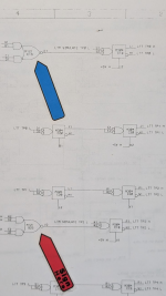
Thinking that if the "LTM SIMULATE TP*" signals are triggered by the manual diagnostic instructions, their counterpart signals should be generated during actual operation. So, we scoped the signal coming out of pin E1 of the M121 in E19 (blue flag) and the signal coming out of pin V2 of the M121 in B25 (red flag). When we run Mark12, E19 E1 falls from high to low, but B25 V2 does not change. There are no pulses that we could detect.

Does this suggest anything meaningful to you? I would have expected to see changes on both pins, and I assumed it would be a repeated sequence of pulses for writing the tape timing track. But the fact that "actual TP3" doesn't change at all seems like a failure.

Zach is retesting all the TC12 flip chips, and we figured we would just keep going "upstream" from these signals... but we don't know if that's a good use of time.

Thoughts? Thanks!
 
Sounds like you're on the right path. Whenever you find an output that doesn't change, immediately check the inputs to see what they're doing. This method is far faster than retesting a bunch of Flip-Chips and allows you to hone in on the problem, rather than using the shotgun approach. You may also be exercising things in such a way in which the tester cannot adequately test for—such as issues related to timing.

You should also be referencing the timing diagrams and ask if what you see in reality looks like what the documentation suggests.
 
You also have to remember that Warren's tester can only tell you that a card is bad. It cannot tell you that a card is good. This is because it cannot provide load testing on an output or marginal voltage on an input. It cannot measure slew rates. The logic when running requires slew rates of a few ns at most and the tester needs many us before it can see if the outputs changed. It is also possible that test vectors are missing some obscure case for the card under test. When it does tell you something is wrong, most likely it is correct. Don't assume that not failing is the same as working correctly.

The good news is that most of the time the failures are not soft so there is good value in testing. But Kyle is correct, follow the logic, don't just blindly retest boards.
 
@ZachyCatGames and I spent a bunch of time today tracing the signals upstream of TP0 and TP3. I'll try to write a report tomorrow, but basically the signals coming from the M304 in C18 seem really weird and inconsistent, including dropping out at time and changing rate, and as far as we could tell, LTS TIMING OK never changed state when starting Mark 12. So it indeed seems that while the diagnostic simulations of TP0 and TP3 work, the actual generation of those signals is not happening.

The timing of the delay chips has not been done at least since when Warren was here... and I was not part of it then. I should have clarified earlier that we have tested recently all the M-series FCs -- but only the ones that did not require a scope. Sometime it would be helpful to get a walkthrough of how to use the FCT with a scope to check those things.

Hopefully more detail tomorrow.
 

Attachments

  • Screenshot_20240920-234302.png
    Screenshot_20240920-234302.png
    221.8 KB · Views: 6
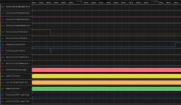
Ok, here's my explanation of what @ZachyCatGames and I saw on Friday.

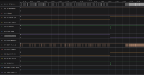
Here's the map of the signals on the machine and the digital channels as they appear on the logic analyzer:
1727018028992.jpeg

Here's what it looks like on the Saleae Logic 16 at 125Ms/s just before and after we push Mark to start the marking process in Mark 12:
1727018125199.png

The first thing one notices is that D16 H1 and E2, the timing signals out of the M304 in C18 are irregular. Putting them next to each other...
1727018253986.png
The short gaps are around 7-12us, but every so often those gaps increase to about 30-40us in a periodic fashion. This might not matter, though, because the signals are not being used until after Mark is pressed.

When Mark is pressed (above image), the timing signals drop out for about 2ms when some other stuff happens (more on that in a second). When the timing signals come back, they start out at about 3.5-4us but quickly settle into about 1.7us intervals:
1727018441791.png
Once they settle, they don't seem to have those irregular gaps as before.

We don't know... maybe the irregular signals (before +0.3ms above) just do that unless they are synced by some process that doesn't happen until the machine is actually trying to mark a tape. If that's the case, then maybe the irregularity before the "mark point" is not a problem, particularly since it seems to settle to a consistent and alternating 1.7us signal once it comes back from the gap between ~0.35ms-0.55ms.

(One thing that occurred to us too late is that there might be signals in those gaps, but they are just sub-threshold. Zach looked at it again captured in analog mode and did not see signals, but we might try again tomorrow for good measure.)

The big thing though, seems to be that D2 (the "real" signal from the top delay that is a kind of proto-TP0) and D10 (the "real" signal from the bottom delay, a proto-TP3) never change, because LTS TIMING OK L never drops. As far as we can tell, it is because those things never happen that the real TP0 and TP3 never happen.

So, it seems like we need to figure out where LTS TIMING OK L comes from, what it's supposed to signify, etc. (Based on the name, we assume it has something to do with the LTS TIMING signals being OK -- just a hunch.)

Any questions or comments welcome, but this is more of a report than a request for help (unless someone sees a mistake in our process or knows what the problem might be). Thanks!
 
Hi all, today @ZachyCatGames and I jumped back into scoping signals on the PDP-12. You may recall that last time we suspected that something was wrong with the LTS TIMING OK signal, because its failure to change meant that the "proto TP0 and TP3" signals were not being emitted from the M112 in D16. We tracked LTS TIMING OK as coming from a big'ol 8-input NAND, namely the M119 in C22:
1727374896656.png
So, today, we used the Saleae to look at that NAND along with the M304s in C18 used to create those proto-signals for TP0 and TP3.
1727375089494.png

First, the solid bars of D10-D13 are the rising and falling signals coming from the M304. They're solid because we're zoomed out too far.

Channels 0-7 are the 8 inputs of the NAND in C22 that generates LTS TIMING OK. They should all be high in order for LTS TIMING OK to be emitted. LCX MARK drops when the Mark switch is pressed. LTD ACIP H rises some time after that, but Mark simply never rises again during this phase. Since LCX MARK stays down, LTS TIMING OK cannot be generated.

We wondered if maybe something was wrong with the logic generating LCX MARK, but looking at old videos where the '12 made it through the first phase of Mark 12 showed that, indeed the Mark light on the console was lit (it is lit when LCX MARK is low). So, it seemed like in the past (at least) we were able to get beyond where we were, even with LCX MARK being low.

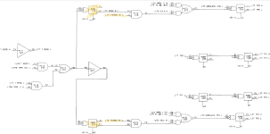
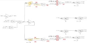
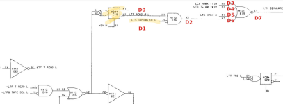
So, we spent some time regrouping. We know that the simulate TP0 and TP3 signals will cause the TAPE WORD FF to be set, and we know that the real TP0 and TP3 signals are not being emitted. In this picture...

1727377128108.png

... we had been focusing on the lower path (labeled D0, D1, D2) for generating TP0 (and the equivalent one for TP3). @ZachyCatGames suggested that we should look more closely at the path for generating TP0/TP3 involving LCX MARK and LTS TC 00 (D3 and D4 here).

It turns out that LTS TC 00 ultimately springs from the M401 in E21 on page 145:

1727375987312.png
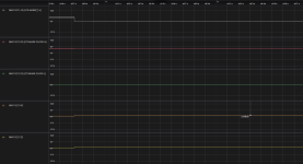
We decided to scope that M401, which hasn't been tested at least since Warren was here, because we don't know how to use the FCT for timing tests. Here's what we saw: (captured using the logic analyzer in analog mode):

1727376315223.png

LCX MARK drops when the Mark switch is pressed, which is what the M401 wants, since it will immediately invert those signals to high, which should start the clock. N2 and S2 appear to be connected as expected (at least, that's what we think that blip is). However, nothing comes out of the clock (channels A4 and A5).

So, we suspect that our M401 is not working. We will look into the documentation for running the timing tests with Warren's FCT and a scope... last time I looked at the readmes I had some questions but I can't remember what they are at the moment.

Thanks for reading -- comments welcome!
 
Last edited:
@ZachyCatGames tells me that there is no FC test for the M401. :cry: How would you folks suggest we proceed testing it?
By understanding what it is supposed to do and checking if it does that. If it doesn't put it on an extender and check the chips in the path to see which one doesn't look right. I assume you don't have a spare so will need to replace the bad parts anyway.

M401 is in the logic handbook which gives a high level description of how it works. From it yes it should be oscillating.
http://www.bitsavers.org/pdf/dec/handbooks/Digital_Logic_Handbook_1972.pdf

Schematics are in various location. Vince has the best collection and frequently has done board layouts which help you find where the chips are. DEC made revisions so ideally need to find one that matches your board. If not pick one that looks close.
https://so-much-stuff.com/pdp8/flipchip/modules.htm

The .brd/.sch files are eagle layout and schematic which you can use to see where the components are. My memory is eagle has gotten less friendly on free level but you can import them into current kicad.

M401 is a challenging one for this method since it uses a lot of discrete components. When transistor circuits get too complex to easily understand it put them in ltspice. Your might be able to find models for the transistors etc with searching but frequently they aren't available. I normally just pick a npn and pnp from whats available with reasonable parameters and it normally is close enough. I haven't needed to simulate ttl gates in ltspice so not sure how difficult they are to simulate.

I think current kicad has tie in to some sort of simulator but I haven't used it.

Since it has two outputs I would first check the second output and see if its dead also.
 
So, yeah, mostly what Dave said. With either J or K (or both) low, D and E should be oscillating at some frequency. D and E should be complements, or something is amiss.

The jumpering from N to S sets the rough order of magnitude for the frequency (17.5 to 175 KHz). The potentiometer should allow you to set the output frequency to whatever it is supposed to be.

If you don't have it in the backplane, you'll also need to supply +5V on A, GND pins C and T, and make the the connection from N to S.

Shouldn't take long to check it out.
 
Thanks, @djg and @vrs42 -- this is all helpful information, thanks. We have never done anything like this before, so this will be a good learning experience. I'm sure we'll have a lot of questions!

In the analog capture above, D2 is high and E2 is low, which is good -- it seems that 1) the signals are able to reach the outputs and 2) whatever is responsible for inverting the signals is working -- but they are not oscillating either before or after the input J2 changes.

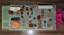
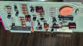
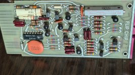
Our M401 has the etch M401H, but there's a stamp on the front that says L... I know that sometimes the same etch is used for different revisions. Is that what the stamp means?

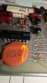
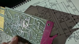
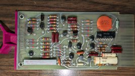
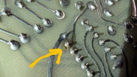
I've attached some pics for reference. One of the pins on the SN7400 looks to me like it may have gotten hot -- but I may just be misinterpreting what I'm seeing.

As an aside, if we do have to replace the SN7400, do you folks recommend adding a socket for future maintenance (if there's space)? It doesn't feel very period, but of course it would make future maintenance easier. Just curious.
 

Attachments

  • PXL_20240927_133553551~2.jpg
    PXL_20240927_133553551~2.jpg
    1.6 MB · Views: 13
  • PXL_20240927_130450251.jpg
    PXL_20240927_130450251.jpg
    3 MB · Views: 12
  • PXL_20240927_130758505.jpg
    PXL_20240927_130758505.jpg
    2.2 MB · Views: 10
  • PXL_20240927_130724539.jpg
    PXL_20240927_130724539.jpg
    2.4 MB · Views: 11
  • PXL_20240927_133322564.jpg
    PXL_20240927_133322564.jpg
    2.2 MB · Views: 11
  • PXL_20240927_130409473.jpg
    PXL_20240927_130409473.jpg
    2.9 MB · Views: 12
  • PXL_20240927_133350286~2.jpg
    PXL_20240927_133350286~2.jpg
    2.5 MB · Views: 13
The darkness on the top side of the indicated IC pin looks like tarnish to me, and there's similar tarnishing on the adjacent pins. The brown stuff on the bottom side looks like flux residue. Maybe a questionable-looking solder joint on that pin was touched up without cleaning the flux afterwards? The appearance of that pin and joint doesn't raise any red flags to me.
 
Back
Top