vrs42
Veteran Member
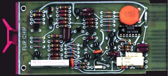
It's an H etch as you identified. I'm not expecting the schematic revision to be an inspection stamp. Instead, the schematic revision is usually pressed into the plastic of the magenta handle.Our M401 has the etch M401H, but there's a stamp on the front that says L... I know that sometimes the same etch is used for different revisions. Is that what the stamp means?
You have a number pressed into the handle, but I don't see a letter there. So I suspect you've got a revision H. Unfortunately, I don't have drawings for the H, and even the L has a second 7400. This means that you'll have to hunt for which pins of which parts do what. Do you have a schematic for revision H?
That doesn't look conclusive to me. The solder may have been reheated to clean up a solder joint.I've attached some pics for reference. One of the pins on the SN7400 looks to me like it may have gotten hot -- but I may just be misinterpreting what I'm seeing.
I'd say it depends on your soldering skills. It they are sketchy, best thing is to clip out the old and install a socket, all the while minimizing the heating time on the pads (while still getting the solder warm enough to flow well). If the available soldering tools and skills are good, there's less concern about damaging the relic, and more about maintaining the original lookAs an aside, if we do have to replace the SN7400, do you folks recommend adding a socket for future maintenance (if there's space)? It doesn't feel very period, but of course it would make future maintenance easier. Just curious.
") .
.